

Click to open expanded view
2.5Gb/s SFP DWDM 40km Optical Transceiver Module
Features
Monitoring interface
Low power dissipation
Up to 2.5Gb/s data links
Single +3.3V power supply
Compliant with SFF-8472
Support Digital Diagnostic
Hot-pluggable SFP footprint
Metal enclosure, for lower EMI
Up to 40km on 9/125µm SMF
RoHS compliant and lead-free
Duplex LC/UPC type pluggable optical interface
DWDM DML laser transmitter and PIN photo-detector
Meet ESD requirements, resist 8KV direct contact voltage
100 GHz ITU channel spacing with integrated wavelength locker
Case operating temperature: Commercial: 0 ~ +70oC
Extended: -10 ~ +80o Industrial: -40 ~ +85oC
Applications
Gigabit Ethernet
C Band DWDM networks
1xFiber /2xFiber Channel
SONET/SDH networks
Wavelength Selection: C-band λc Wavelength Guide Pin Descriptions
|
Channel |
Wavelength (nm) |
Frequency (THZ) |
Channel |
Wavelength (nm) |
Frequency (THZ) |
|
C17 |
1563.86 |
191.70 |
C39 |
1546.12 |
193.90 |
|
C18 |
1563.05 |
191.80 |
C40 |
1545.32 |
194.00 |
|
C19 |
1562.23 |
191.90 |
C41 |
1544.53 |
194.10 |
|
C20 |
1561.42 |
192.00 |
C42 |
1543.73 |
194.20 |
|
C21 |
1560.61 |
192.10 |
C43 |
1542.94 |
194.30 |
|
C22 |
1559.79 |
192.20 |
C44 |
1542.14 |
194.40 |
|
C23 |
1558.98 |
192.30 |
C45 |
1541.35 |
194.50 |
|
C24 |
1558.17 |
192.40 |
C46 |
1540.56 |
194.60 |
|
C25 |
1557.36 |
192.50 |
C47 |
1539.77 |
194.70 |
|
C26 |
1556.55 |
192.60 |
C48 |
1538.98 |
194.80 |
|
C27 |
1555.75 |
192.70 |
C49 |
1538.19 |
194.90 |
|
C28 |
1554.94 |
192.80 |
C50 |
1537.40 |
195.00 |
|
C29 |
1554.13 |
192.90 |
C51 |
1536.61 |
195.10 |
|
C30 |
1553.33 |
193.00 |
C52 |
1535.82 |
195.20 |
|
C31 |
1552.52 |
193.10 |
C53 |
1535.04 |
195.30 |
|
C32 |
1551.72 |
193.20 |
C54 |
1534.25 |
195.40 |
|
C33 |
1550.92 |
193.30 |
C55 |
1533.47 |
195.50 |
|
C34 |
1550.12 |
193.40 |
C56 |
1532.68 |
195.60 |
|
C35 |
1549.32 |
193.50 |
C57 |
1531.90 |
195.70 |
|
C36 |
1548.51 |
193.60 |
C58 |
1531.12 |
195.80 |
|
C37 |
1547.72 |
193.70 |
C59 |
1530.33 |
195.90 |
|
C38 |
1546.92 |
193.80 |
C60 |
1529.55 |
196.00 |
|
Non-ITU |
Peak wavelength between 1528.77nm-1563.86 |
C61 |
1528.77 |
196.10 |
|
Absolute Maximum Ratings
It has to be noted that the operation in excess of any individual absolute maximum ratings might cause permanent damage to this module.
|
Parameter |
Symbol |
Min |
Max |
Unit |
Notes |
|
Storage Temperature |
TS |
-40 |
85 |
oC |
|
|
Power Supply Voltage |
VCC |
-0.5 |
3.6 |
V |
|
|
Relative Humidity (non-condensation) |
RH |
5 |
95 |
% |
|
|
Damage Threshold |
THd |
0 |
dBm |
Recommended Operating Conditions and Power Supply Requirements
|
Parameter |
Symbol |
Min |
Typical |
Max |
Unit |
Notes |
|
Operating Case Temperature |
TOP |
0 |
70 |
oC |
commercial |
|
|
-10 |
80 |
extended |
||||
|
-40 |
85 |
industrial |
||||
|
Power Supply Voltage |
VCC |
3.135 |
3.3 |
3.465 |
V |
|
|
Data Rate |
2.5 |
Gb/s |
||||
|
Control Input Voltage High |
2 |
Vcc |
V |
|||
|
Control Input Voltage Low |
0 |
0.8 |
V |
|||
|
Link Distance (SMF) |
D |
40 |
km |
9/125um |
General Description
HC-2Lxx41x transceivers include an PIN photo-detector diode and temperature stabilized DWDM DML transmitter. Digital diagnostic functions are available via an I2C.This module is designed for single mode fiber and operates at a nominal wavelength of 100GHz ITU Grid, C Band DWDM wavelength. Digital diagnostics functions are available via a 2-wire serial interface, as specified in SFF-8472.
The optical output can be disabled by a TTL logic high-level input of Tx Disable, and the system also can disable the module via I2C. Tx Fault is provided to indicate that degradation of the laser. Loss of signal (LOS) output is provided to indicate the loss of an input optical signal of receiver or the link status with partner. The system can also get the LOS (or Link)/Disable/Fault information via I2C register access.
Pin Assignment and Pin Description
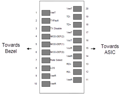
Figure1. Diagram of host board connector block pin numbers and names
|
PIN |
Name |
Name/Description |
Notes |
|
1 |
VEET |
Transmitter Ground (Common with Receiver Ground) |
1 |
|
2 |
TXFAULT |
Transmitter Fault. |
|
|
3 |
TXDIS |
Transmitter Disable. Laser output disabled on high or open. |
2 |
|
4 |
MOD_DEF(2) |
Module Definition 2. Data line for Serial ID. |
3 |
|
5 |
MOD_DEF(1) |
Module Definition 1. Clock line for Serial ID. |
3 |
|
6 |
MOD_DEF(0) |
Module Definition 0. Grounded within the module. |
3 |
|
7 |
Rate Select |
No connection required |
4 |
|
8 |
LOS |
Loss of Signal indication. Logic 0 indicates normal operation. |
5 |
|
9 |
VEER |
Receiver Ground (Common with Transmitter Ground) |
1 |
|
10 |
VEER |
Receiver Ground (Common with Transmitter Ground) |
1 |
|
11 |
VEER |
Receiver Ground (Common with Transmitter Ground) |
1 |
|
12 |
RD- |
Receiver Inverted DATA out. AC Coupled |
|
|
13 |
RD+ |
Receiver Non-inverted DATA out. AC Coupled |
|
|
14 |
VEER |
Receiver Ground (Common with Transmitter Ground) |
1 |
|
15 |
VCCR |
Receiver Power Supply |
|
|
16 |
VCCT |
Transmitter Power Supply |
|
|
17 |
VEET |
Transmitter Ground (Common with Receiver Ground) |
1 |
|
18 |
TD+ |
Transmitter Non-Inverted DATA in. AC Coupled. |
|
|
19 |
TD- |
Transmitter Inverted DATA in. AC Coupled. |
|
|
20 |
VEET |
Transmitter Ground (Common with Receiver Ground) |
1 |
Notes:
1. Circuit ground is internally isolated from chassis ground.
2. Laser output disabled on TDIS >2.0V or open, enabled on TDIS<0.8V.
3. Should be pulled up with 4.7k-10k ohms on host board to a voltage between 2.0V and 3.6V.MOD_DEF (0) pulls line low to indicate module is plugged in.
4. This is an optional input used to control the receiver bandwidth for compatibility with multiple data rates (most likely Fiber Channel 1x and 2x Rates).If implemented, the input will be internally pulled down with > 30kΩ resistor. The input states are:
1) Low (0 – 0.8V): Reduced Bandwidth
2) (>0.8, < 2.0V): Undefined
3) High (2.0 – 3.465V): Full Bandwidth
4) Open: Reduced Bandwidth
5. LOS is open collector output should be pulled up with 4.7k-10k ohms on host board to a voltage between 2.0V and 3.6V. Logic 0 indicates normal operation; logic 1 indicates loss of signal.
Specification of Transmitter Electrical Characteristics
The following electrical characteristics are defined over the Recommended Operating Environment unless otherwise specified.
|
Parameter |
Symbol |
Min. |
Typical |
Max |
Unit |
Notes |
|
|
Power Consumption |
1.0 |
W |
commercial |
||||
|
1.5 |
Industrial |
||||||
|
Supply Current |
Icc |
300 |
mA |
commercial |
|||
|
450 |
Industrial |
||||||
|
Transmitter |
|||||||
|
Single-ended Input Voltage Tolerance |
-0.3 |
4.0 |
V |
||||
|
Differential Input Voltage Swing |
Vin,pp |
200 |
2400 |
mVpp |
|||
|
Differential Input Impedance |
Zin |
90 |
100 |
110 |
Ohm |
||
|
Transmit Disable Assert Time |
5 |
us |
|||||
|
Transmit Disable Voltage |
Vdis |
Vcc-1.3 |
Vcc |
V |
|||
|
Transmit Enable Voltage |
Ven |
Vee-0.3 |
0.8 |
V |
|||
|
Receiver |
|||||||
|
Differential Output Voltage Swing |
Vout,pp |
500 |
900 |
mVpp |
|||
|
Differential Output Impedance |
Zout |
90 |
100 |
110 |
Ohm |
||
|
Data output rise/fall time |
Tr/Tf |
100 |
ps |
20% to 80% |
|||
|
LOS Assert Voltage |
VlosH |
Vcc-1.3 |
Vcc |
V |
|||
|
LOS De-assert Voltage |
VlosL |
Vee-0.3 |
0.8 |
V |
|||
Optical Characteristics
The following optical characteristics are defined over the Recommended Operating Environment unless otherwise specified.
|
Parameter |
Symbol |
Min. |
Typical |
Max |
Unit |
Notes |
|
Transmitter |
||||||
|
Optical Wavelength |
λC |
λc -0.1 |
λc +0.1 |
nm |
1 |
|
|
Center Wavelength Spacing |
100 |
GHz |
||||
|
Spectrum Bandwidth(RMS) |
σ |
1 |
nm |
|||
|
Side Mode Suppression Ratio |
SMSR |
30 |
dB |
|||
|
Average Optical Power |
PAVG |
-2 |
3 |
dBm |
2 |
|
|
Optical Extinction Ratio |
ER |
8.2 |
dB |
|||
|
Transmitter OFF Output Power |
POff |
-45 |
dBm |
|||
|
Transmitter Eye Mask |
Compliant with G.957(class 1 laser safety) |
|||||
|
Receiver |
||||||
|
Center Wavelength |
λC |
1270 |
1610 |
nm |
||
|
Receiver Sensitivity (Average Power) |
Sen. |
-19 |
dBm |
3 |
||
|
Input Saturation Power (overload) |
Psat |
0 |
dBm |
|||
|
LOS Assert |
LOSA |
-36 |
dB |
4 |
||
|
LOS De-assert |
LOSD |
-20 |
dBm |
4 |
||
|
LOS Hysteresis |
LOSH |
0.5 |
2 |
6 |
dBm |
|
Notes:
1. λc refer to wavelength selection, and corresponds to approximately 0.8 nm
2. Measure at 2^23-1 NRZ PRBS pattern
3. Measured with Light source 1563.86~1528.77nm, ER=8.2dB; BER =<10^-12 @PRBS=2^23-1 NRZ
4. When LOS de-asserted, the RX data+/- output is High-level (fixed).
Mechanical Dimensions
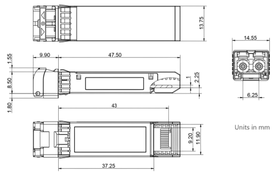
Figure2. Mechanical Outline
If you need more support , Please contact us .
