

Click to open expanded view
1.25Gb/s SFP CWDM 40km
Product Features
Ø Up to 1.25Gb/s Data Links
Ø Hot-Pluggable
Ø Duplex LC connector
Ø Up to 40km on 9/125μm SMF
Ø 18-Wavelength CWDM 1270n~1610nm Available
Ø CWDM DFB laser transmitter
Ø Single +3.3V Power Supply
Ø Monitoring Interface Compliant with SFF-8472
Ø Low power dissipation <1W typically
Ø Operating temperature range: -20°C to 85°C
Ø RoHS compliant and Lead Free
Applications
Ø Gigabit Ethernet
Ø 1XFiber Channel
Ø CWDM Networks
Description
HC-1.25G-CXXL-40D-I is a high-performance, cost-effective module that supports data rates up to 1.25 Gbps over single-mode fiber with a transmission distance of up to 40 km. The transceiver's serial EEPROM allows users to access transceiver monitoring and configuration data via a two-wire SFP management interface. The transceiver consists of two sections: the transmit section includes a laser driver and a CWDM DFB laser. The receive section includes a PIN photodiode with an integrated transimpedance preamplifier (TIA) and limiting amplifier. The product offers 18 center wavelengths ranging from 1270 nm to 1610 nm. The 20 nm channel spacing enables uncooled laser operation, high-yield manufacturing processes, and low-cost multiplexing/demultiplexing techniques, providing a complete and cost-effective solution for a variety of data and telecommunications applications.
Absolute Maximum Ratings
Table 2-Absolute Maximum Ratings
|
Parameter |
Symbol |
Min |
Max |
Unit |
Note |
|
Storage Temperature |
TS |
-40 |
85 |
°C |
|
|
Operating Case Temperature |
TOP |
-20 |
85 |
°C |
|
|
Power Supply Voltage |
VCC |
-0.5 |
3.6 |
V |
|
|
Relative Humidity (non-condensation) |
RH |
0 |
85 |
% |
|
Note:
It has to be noted that the operation in excess of any individual absolute maximum ratings might cause permanent damage to this module
Recommended Operating Conditions
Table 3-Recommended Operating Conditions
|
Parameter |
Symbol |
Min |
Typical |
Max |
Unit |
Note |
|
Operating Case Temperature |
TOP |
-20 |
|
85 |
°C |
|
|
Power Supply Voltage |
VCC |
3.135 |
3.3 |
3.465 |
V |
|
|
Power Consumption |
P |
|
|
1 |
W |
|
|
Supply Current |
Icc |
|
|
300 |
mA |
|
|
Bit Error Rate |
BER |
|
|
10-12 |
|
|
|
Aggregate Bit Rate |
BRAVE |
- |
1.25 |
- |
Gb/s |
|
|
Transmission Distance |
TD |
|
- |
80 |
KM |
Over SMF |
Optical Characteristics
Table 4-Optical Characteristics
|
Transmitter Optical Specification |
||||||
|
Parameter |
Symbol |
Min |
Typ |
Max |
Units |
Notes |
|
Center Wavelength |
λc |
λ-6.5 |
λ |
λ+6.5 |
nm |
|
|
Spectral Width |
σ |
|
|
1 |
nm |
|
|
Side Mode Suppression Ratio |
SMSR |
30 |
|
|
dB |
|
|
Optical Output Power |
Pout |
-5 |
|
0 |
dBm |
|
|
Optical Rise/Fall Time |
tr / tf |
|
|
260 |
ps |
|
|
Extinction Ratio |
ER |
8.2 |
|
|
dB |
|
|
Generated Jitter (peak to peak) |
JTXp-p |
|
|
0.07 |
UI |
|
|
Generated Jitter (rms) |
JTXrms |
|
|
0.007 |
UI |
|
|
Eye Mask for Optical Output |
|
Compliant with IEEE802.3z(class 1 laser safety) |
|
|
||
|
Receiver Optical Specification |
||||||
|
Optical Input Wavelength |
λc |
1460 |
|
1620 |
nm |
|
|
Receiver Overload |
Pol |
+3 |
|
|
dBm |
|
|
RX Sensitivity |
Sen |
|
|
-24 |
dBm |
|
|
RX_LOS Assert |
LOS A |
-35 |
|
|
dBm |
|
|
RX_LOS De-assert |
LOS D |
|
|
-27 |
dBm |
|
|
RX_LOS Hysteresis |
LOS H |
0.5 |
|
|
dB |
|
Electrical Characteristics
The following electrical characteristics are defined over the recommended operating environment
Table 5-Electrical Characteristics
|
Parameter |
Symbol |
Min |
Typ |
Max |
Units |
Notes |
|
Transmitter (Module Input) |
||||||
|
Input differential impedance |
Rin |
90 |
100 |
110 |
|
|
|
Single ended data input swing |
Vin PP |
250 |
|
1200 |
mVp-p |
1 |
|
Transmit Disable Voltage |
VD |
Vcc – 1.3 |
|
Vcc |
V |
2 |
|
Transmit Enable Voltage |
VEN |
Vee |
|
Vee+ 0.8 |
V |
|
|
Transmit Disable Assert Time |
Tdessert |
|
|
10 |
us |
|
|
Receiver (Module Output) |
||||||
|
Single ended data output swing |
Vout,pp |
300 |
|
800 |
mv |
3 |
|
Data output rise time |
tr |
|
|
260 |
ps |
4 |
|
Data output fall time |
tf |
|
|
260 |
ps |
4 |
|
LOS Fault |
Vlosfault |
Vcc – 0.5 |
|
VCC_host |
V |
5 |
|
LOS Normal |
Vlos norm |
Vee |
|
Vee+0.5 |
V |
5 |
|
Power Supply Rejection |
PSR |
100 |
|
|
mVpp |
6 |
Note:
1、 AC coupled.
2、 Or open circuit.
3、 Into 100 ohm differential termination. 4. 20 – 80 %
4、 LOS is LVTTL. Logic 0 indicates normal operation; logic 1 indicates no signal detected.
5、 All transceiver specifications are compliant with a power supply sinusoidal modulation of 20 Hz to
1.5MHz up to specified value applied through the power supply filtering network shown on page 23 of the Small Form-factor Pluggable (SFP) Transceiver Multi-Source Agreement (MSA), September 14, 2000
Digital Diagnostics
Table 6-Digital Diagnostics
|
Parameter |
Symbol |
Min |
Max |
Unit |
Note |
|
Temperature Monitor Absolute Error |
DMI_Temp |
-3 |
3 |
°C |
Cover full operating temperature range |
|
Supply Voltage Monitor Absolute Error |
DMI _VCC |
-0.1 |
0.1 |
V |
Cover full operating temperature range |
|
Channel RX Power Monitor Absolute Error |
DMI_RX_Ch |
-3 |
3 |
dB |
|
|
Channel Bias Current Monitor |
DMI_Ibias_Ch |
-10% |
10% |
|
|
|
Channel TX Power Monitor Absolute Error |
DMI_TX_Ch |
-3 |
3 |
dB |
|
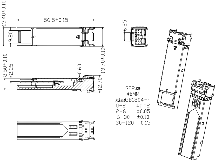
Mechanical Dimension
If you need more support , Please contact us .
