

Click to open expanded view
100Gbps QSFP28 BIDI Transceiver, 80KM Reach
Product Features
Ø Simplex LC connector·
Ø RoHS Compliant Part
Ø Single +3.3V power supply operating
Ø 4x25Gb/s LAN WDM Blue or Red Side TOSA, LAN WDM Red or Blue Side ROSA with SOA
Ø Support 100GBASE-BIDI for line rate of 103.125Gbps and OTU4 for line rate of 111.81Gbps
Ø Compliant with IEEE 802.3-2012 Clause 88 standard IEEE 802.3bm CAUI-4 chip to module electrical standard ITU-T G.959.1-2012-02 standard
Ø Temperature range commercial grade: 0~+70℃ , industrial grade: - 40 ~85℃
Applications
Ø 100G BASE Ethernet
Ø Data center network
Description
This transceiver provides 100GBase-BX throughput up to 80km over single-mode fiber (SMF) using wavelengths of 1273.54, 1277.89, 1282.26, 1286.66nm- TX/1295.56, 1300.05, 1304.58, 1309.14nm-RX(1295.56, 1300.05, 1304.58, 1309.14nm- TX/1273.54, 1277.89, 1282.26, 1286.66nm-RX) via an LC connector. This bidirectional unit must be used with another transceiver or network appliance of complimenting wavelengths. Digital diagnostics functions are also available via the I2C interface, as specified by the QSFP28 MSA, to allow access to real-time operating parameters. With these features, this easy to install, hot swappable transceiver is suitable to be used in various applications, such as 100G Ethernet, data center, and storage area networks applications.
Absolute Maximum Ratings
It has to be noted that the operation in excess of any individual absolute maximum ratings might cause permanent damage to this module.
Table 1-Absolute Maximum Ratings
|
Parameter |
Symbol |
Min |
Max |
Unit |
Note |
|
Storage Temperature |
TS |
-40 |
85 |
°C |
|
|
Operating Case Temperature |
TOP |
0 |
70 |
°C |
|
|
Power Supply Voltage |
VCC |
-0.5 |
4 |
V |
|
|
Relative Humidity (non-condensation) |
RH |
0 |
85 |
% |
|
Recommended Operating Conditions
Table 2 -Recommended Operating Conditions
|
Parameter |
Symbol |
Min |
Typical |
Max |
Unit |
Note |
|
Operating Case Temperature |
TOP |
0 |
|
70 |
°C |
|
|
Power Supply Voltage |
VCC |
3.135 |
3.3 |
3.465 |
V |
|
|
Power Consumption |
|
|
|
6.5 |
W |
|
|
Supply Current |
Icc |
|
1200 |
1800 |
mA |
|
|
BRAVE |
- |
103.125 |
- |
Gb/s |
|
|
|
Transmission Distance |
TD |
|
- |
80 |
KM |
Over SMF |
Optical Characteristics
Table 3 -Optical Characteristics
|
Parameter |
Symbol |
Min |
Typ |
Max |
Unit |
Note |
|
Transmitter |
||||||
|
Blue Side Four Lane Wavelength Range
|
l1 |
1272.54 |
1273.54 |
1274.54 |
nm |
|
|
l2 |
1276.89 |
1277.89 |
1278.89 |
nm |
|
|
|
l3 |
1281.25 |
1282.26 |
1283.27 |
nm |
|
|
|
l4 |
1285.65 |
1286.66 |
1287.68 |
nm |
|
|
|
Red Side Four Lane Wavelength Range
|
l1 |
1294.56 |
1295.56 |
1296.56 |
nm |
|
|
l2 |
1299.05 |
1300.05 |
1301.05 |
nm |
|
|
|
l3 |
1303.58 |
1304.58 |
1305.58 |
nm |
|
|
|
l4 |
1308.14 |
1309.14 |
1310.14 |
nm |
|
|
|
Side-mode Suppression Ratio |
SMSR |
30 |
- |
- |
dB |
|
|
Total Average Launch Power |
PT |
8 |
- |
12.5 |
dBm |
|
|
Average Launch Power, each Lane |
|
+2 |
- |
6.5 |
dBm |
|
|
Difference in Launch Power between any two Lanes (OMA) |
|
- |
- |
3 |
dB |
|
|
Extinction Ratio |
ER |
6 |
- |
- |
dB |
|
|
Transmitter Eye Mask Definition {X1, X2, X3, Y1, Y2, Y3} |
|
{0.25, 0.4, 0.45, 0.25, 0.28, 0.4} |
|
|
||
|
Optical Return Loss Tolerance |
|
- |
- |
20 |
dB |
|
|
Average Launch Power OFF Transmitter, each Lane |
Poff |
|
|
-30 |
dBm |
|
|
Relative Intensity Noise |
Rin |
|
|
-130 |
dB/HZ |
|
|
Optical return loss tolerance |
|
|
|
20 |
dB |
|
|
Transmitter reflectance |
|
- |
- |
12 |
dB |
|
|
Receiver |
||||||
|
Red Side Four Lane Wavelength Range
|
l1 |
1272.54 |
1273.54 |
1274.54 |
nm |
|
|
l2 |
1276.89 |
1277.89 |
1278.89 |
nm |
|
|
|
l3 |
1281.25 |
1282.26 |
1283.27 |
nm |
|
|
|
l4 |
1285.65 |
1286.66 |
1287.68 |
nm |
|
|
|
Blue Side Four Lane Wavelength Range
|
l1 |
1294.56 |
1295.56 |
1296.56 |
nm |
|
|
l2 |
1299.05 |
1300.05 |
1301.05 |
nm |
|
|
|
l3 |
1303.58 |
1304.58 |
1305.58 |
nm |
|
|
|
l4 |
1308.14 |
1309.14 |
1310.14 |
nm |
|
|
|
Total Damage Threshold |
THd |
|
|
5.5 |
dBm |
|
|
Receiver Sensitivity per Lane |
R |
|
|
-28 |
dBm |
|
|
Average Power at Receiver Input, each Lane |
R |
-28 |
|
0 |
dBm |
|
|
LOS De-Assert |
LOSD |
|
|
-29 |
dBm |
|
|
LOS Assert |
LOSA |
-40 |
|
|
dBm |
|
|
LOS Hysteresis |
LOSH |
0.5 |
|
|
dB |
|
Electrical Characteristics
Table 4 -Electrical Characteristics
The following electrical characteristics are defined over the recommended operating environment
|
Parameter |
Symbol |
Min |
Typ |
Max |
Unit |
Note |
||
|
Data Rate per Channel |
|
- |
25.78125 |
|
Gbps |
|
||
|
|
27.9525 |
|
|
|||||
|
Power Consumption |
|
- |
4 |
6.5 |
W |
|
||
|
Supply Current |
Icc |
|
1.2 |
1.8 |
A |
|
||
|
Control I/O Voltage-High |
VIH |
2.0 |
|
Vcc |
V |
|
||
|
Control I/O Voltage-Low |
VIL |
0 |
|
0.7 |
V |
|
||
|
Inter-Channel Skew |
TSK |
|
|
35 |
Ps |
|
||
|
RESETL Duration |
|
|
10 |
|
Us |
|
||
|
RESETL De-assert time |
|
|
|
100 |
ms |
|
||
|
Power On Time |
|
|
|
100 |
ms |
|
||
|
Transmitter |
||||||||
|
Single Ended Output Voltage Tolerance |
|
0.3 |
|
Vcc |
V |
|
||
|
Common mode Voltage Tolerance |
|
15 |
|
|
mV |
|
||
|
Transmit Input Diff Voltage |
VI |
150 |
|
1200 |
mV |
|
||
|
Transmit Input Diff Impedance |
ZIN |
85 |
100 |
115 |
|
|
||
|
Data Dependent Input Jitter |
DDJ |
|
0.3 |
|
UI |
|
||
|
Receiver |
||||||||
|
Single Ended Output Voltage Tolerance |
|
0.3 |
|
4 |
V |
|
||
|
Rx Output Diff Voltage |
Vo |
370 |
600 |
950 |
mV |
|
||
|
Rx Output Rise and Fall Voltage |
Tr/Tf |
|
|
35 |
ps |
|
||
|
Total Jitter |
TJ |
|
0.3 |
|
UI |
|
||
Digital Diagnostics
Table 5 -Digital Diagnostics
|
Parameter |
Symbol |
Min |
Max |
Unit |
Note |
|
Temperature Monitor Absolute Error |
DMI_Temp |
-3 |
3 |
°C |
Cover full operating temperature range |
|
Supply Voltage Monitor Absolute Error |
DMI _VCC |
-0.1 |
0.1 |
V |
Cover full operating temperature range |
|
Channel RX Power Monitor Absolute Error |
DMI_RX_Ch |
-3 |
3 |
dB |
|
|
Channel Bias Current Monitor |
DMI_Ibias_Ch |
-10% |
10% |
|
|
|
Channel TX Power Monitor Absolute Error |
DMI_TX_Ch |
-3 |
3 |
dB |
|
Edge connector and pinout description
The electrical pinout of the QSFP28 module is shown in Figure 1 below.
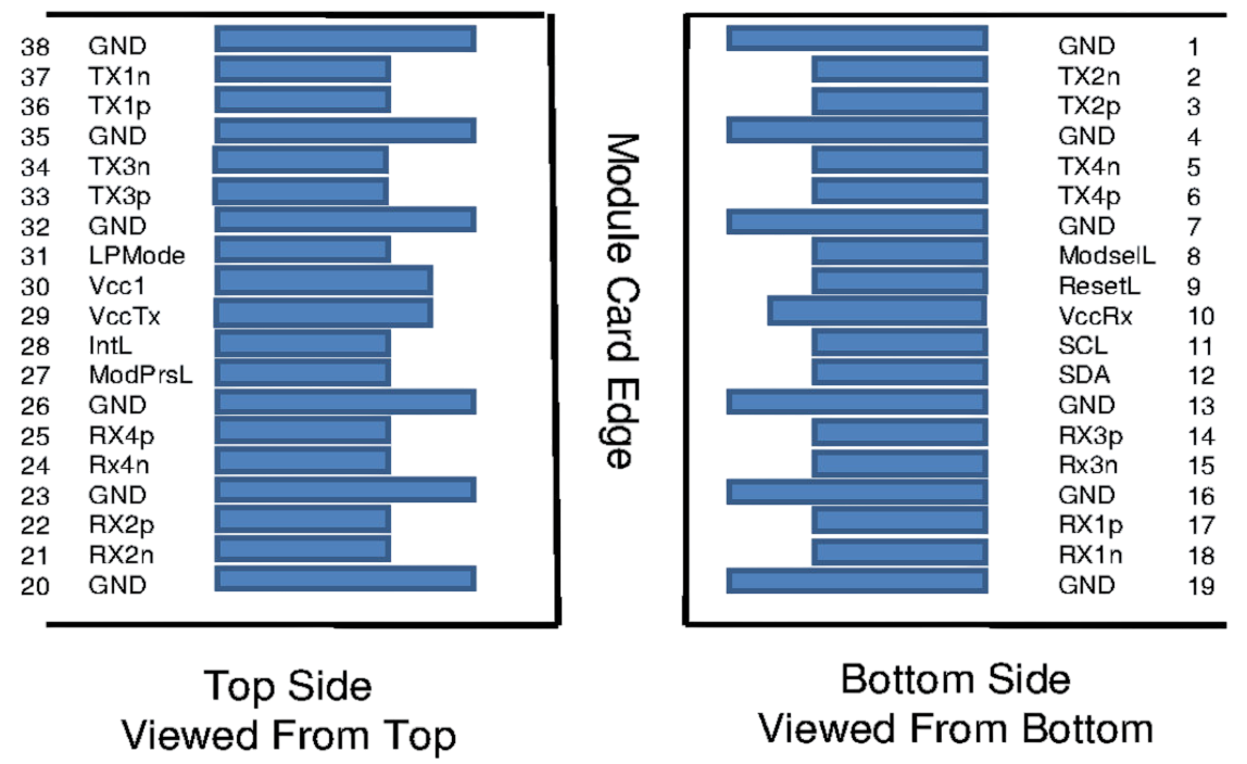
|
Pin |
Symbol |
Name/Description |
Notes |
|
1 |
GND |
Transmitter Ground |
1 |
|
2 |
Tx2n |
Transmitter Inverted Data Input |
|
|
3 |
Tx2p |
Transmitter Non-Inverted Data output |
|
|
4 |
GND |
Transmitter Ground |
1 |
|
5 |
Tx4n |
Transmitter Inverted Data Input |
|
|
6 |
Tx4p |
Transmitter Non-Inverted Data output |
|
|
7 |
GND |
Transmitter Ground |
1 |
|
8 |
ModSelL |
Module Select |
|
|
9 |
ResetL |
Module Reset |
|
|
10 |
VccRx |
3.3V Power Supply Receiver |
2 |
|
11 |
SCL |
2-Wire serial Interface Clock |
|
|
12 |
SDA |
2-Wire serial Interface Data |
|
|
13 |
GND |
Receiver Ground |
1 |
|
14 |
Rx3p |
Receiver Non-Inverted Data Output |
|
|
15 |
Rx3n |
Receiver Inverted Data Output |
|
|
16 |
GND |
Receiver Ground |
1 |
|
17 |
Rx1p |
Receiver Non-Inverted Data Output |
|
|
18 |
Rx1n |
Receiver Inverted Data Output |
|
|
19 |
GND |
Receiver Ground |
1 |
|
20 |
GND |
Receiver Ground |
1 |
|
21 |
Rx2n |
Receiver Inverted Data Output |
|
|
22 |
Rx2p |
Receiver Non-Inverted Data Output |
|
|
23 |
GND |
Receiver Ground |
1 |
|
24 |
Rx4n |
Receiver Inverted Data Output |
|
|
25 |
Rx4p |
Receiver Non-Inverted Data Output |
|
|
26 |
GND |
Receiver Ground |
1 |
|
27 |
ModPrsl |
Module Present |
|
|
28 |
IntL |
Interrupt |
|
|
29 |
VccTx |
3.3V power supply transmitter |
2 |
|
30 |
Vcc1 |
3.3V power supply |
2 |
|
31 |
LPMode |
Low Power Mode,not connect |
|
|
32 |
GND |
Transmitter Ground |
1 |
|
33 |
Tx3p |
Transmitter Non-Inverted Data Input |
|
|
34 |
Tx3n |
Transmitter Inverted Data Output |
|
|
35 |
GND |
Transmitter Ground |
1 |
|
36 |
Tx1p |
Transmitter Non-Inverted Data Input |
|
|
37 |
Tx1n |
Transmitter Inverted Data Output |
|
|
38 |
GND |
Transmitter Ground |
1 |
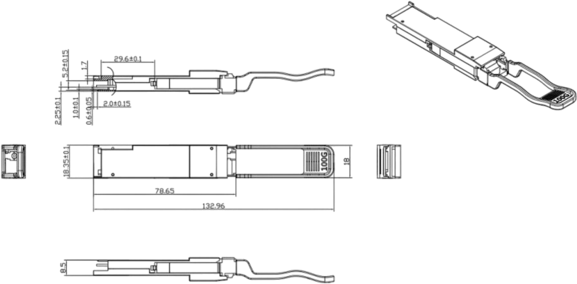
Mechanical Dimension
If you need more support , Please contact us .
