


Thin Film lithium niobate IQ Modulator
This device features thermal-optic bias control interface and is manufactured using advanced coupling and micro-electronic processes, and realizes high opto-electric conversion efficiency on TFLN. Our products provide superior characteristics on half-wave voltage, stability, and device size, significantly enhancing critical performance in digital optical communications and telecommunication networks.
Product Description
C-band TFLN 20/30/40 GHz IQ modulator device.
Features
Bandwidth up-to 40 GHz
Low half-wave voltage 3.5 V
Low insertion loss ≤ 8 dB
Specifications
|
Category |
Parameters |
Symbol |
Unit |
Performance |
||
|
Optical Features |
Operating Wavelength |
λ |
nm |
~1550 |
||
|
Optical Extinction Ratio (@ DC) |
ER |
dB |
≥ 20 |
|||
|
Optical Return Loss |
ORL |
dB |
≤ -27 |
|||
|
Optical Insertion Loss (*) |
IL |
dB |
≤ 8 |
|||
|
Electrical Features |
3 dB Bandwidth (from 2 GHz) |
S21 |
GHz |
X1: 2 |
X1: 3 |
X1: 4 |
|
Min: 18 Typ: 20 |
Min: 26 Typ: 30 |
Min: 36 Typ: 40 |
||||
|
Child RF Vπ (@ 50 kHz) |
Vπ-C |
V |
3 ~ 3.5 |
|||
|
Heater Resistance |
Rh |
Ohm |
4000 ± 10% |
|||
|
Heater Pπ(@ DC) |
Pπ |
mw |
≤ 40 |
|||
|
RF Return Loss (10 MHz to 40 GHz) |
S11 |
dB |
≤ -10 |
|||
|
Work Condition |
Operating Temperature |
TO |
°C |
-10~60 |
||
- Lower insertion loss is available for customization.
Absolute Maximum Ratings
Working over maximum ratings could significantly reduce device reliability and cause irreversible damage.
|
Parameters |
Symbol |
Min. |
Max. |
Unit |
|
RF Input Power (*) |
Sin |
- |
23 |
dBm |
|
RF Swing Voltage (*) |
Vpp |
- |
8.93 |
V |
|
RF RMS Voltage (*) |
Vrms |
- |
3.16 |
V |
|
Heater Bias Voltage |
Uheater |
- |
15 |
V |
|
Storage Temperature |
Ts |
-40 |
85 |
℃ |
|
Relative Humidity (no condensation) |
RH |
5 |
90 |
% |
* Higher RF input power is customizable.
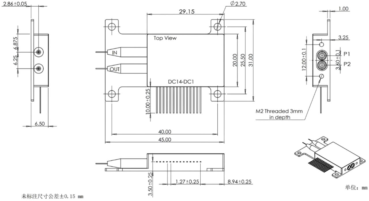
Package and Pins (Unit: mm)
|
PIN |
Symbol |
Description |
PIN |
Symbol |
Description |
|
RF1 |
P1 |
RF Input “I” |
7 |
DC7 |
Parent MZM bias2 |
|
RF2 |
P2 |
RF Input “Q” |
8 |
DC8 |
N/A |
|
1 |
DC1 |
N/A |
9 |
DC9 |
P MZM MPD anode |
|
2 |
DC2 |
I1(Child MZM I) bias |
10 |
DC10 |
P MZM MPD cathode |
|
3 |
DC3 |
I2(Child MZM I) bias |
11 |
DC11 |
Q MZM MPD anode |
|
4 |
DC4 |
Q1(Child MZM Q) bias |
12 |
DC12 |
Q MZM MPD cathode |
|
5 |
DC5 |
Q2(Child MZM Q) bias |
13 |
DC13 |
I MZM MPD anode |
|
6 |
DC6 |
Parent MZM bias1 |
14 |
DC14 |
I MZM MPD cathode |
Notes:
1. Both input and output are PM fibers, FC/APC connectors.
2. RF adaptor type is SSMP (i.e. SMPM or GPPO).
S21 Measurement (20GHz Typical)
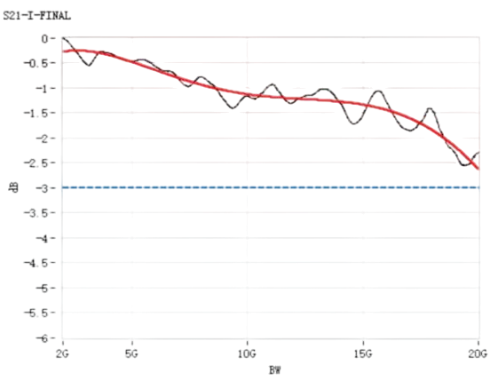
Figure : S21
Ordering Information : HC-X1C8PPBC61
|
Optional Model |
Description |
Optional Code |
|
X1 |
RF 3dB Bandwidth |
2 or 3 or 4 |
