

Click to open expanded view
25Gb/s SFP28 850nm 100m Transceiver
Features
Up to 25Gb/s data links
Single +3.3V power supply
Hot-pluggable SFP footprint
Class 1 laser safety certified
Up to 100m on 50/125um MMF
RoHS-10 compliant and lead-free
Support Digital Monitoring interface
850nm VCSEL laser and PIN receiver
All-metal housing for superior EMI performance
Cost effective SFP28 solution, enables higher port densities and greater bandwidth
2-wire interface for management specifications compliant with SFF 8472 digital diagnostic monitoring interface for optical transceivers
Case operating temperature Commercial: 0 ~ +70oC Extended: -10 ~ +80oC Industrial: -40 ~ +85oC
Applications
Other Optical Links
Inter Rack Connection
Custom high-speed data pipes
Computer cluster cross-connect
High-speed storage area networks
Absolute Maximum Ratings
It has to be noted that the operation in excess of any individual absolute maximum ratings might cause permanent damage to this module.
|
Parameter |
Symbol |
Min |
Max |
Unit |
Notes |
|
Storage Temperature |
TS |
-40 |
85 |
oC |
|
|
Power Supply Voltage |
VCC |
-0.5 |
3.6 |
V |
|
|
Relative Humidity (non-condensation) |
RH |
5 |
95 |
% |
|
|
Damage Threshold |
THd |
3.4 |
dBm |
Recommended Operating Conditions
|
Parameter |
Symbol |
Min |
Typical |
Max |
Unit |
Notes |
|
Operating Case Temperature |
TOP |
0 |
70 |
oC |
commercial |
|
|
-10 |
80 |
Extended |
||||
|
-40 |
85 |
Industrial |
||||
|
Power Supply Voltage |
VCC |
3.135 |
3.3 |
3.465 |
V |
|
|
Data Rate |
25 |
Gb/s |
||||
|
Control Input Voltage High |
2 |
Vcc |
V |
|||
|
Control Input Voltage Low |
0 |
0.8 |
V |
|||
|
Link Distance (MMF) |
D |
100 |
m |
50/125um |
Pin Assignment and Pin Description
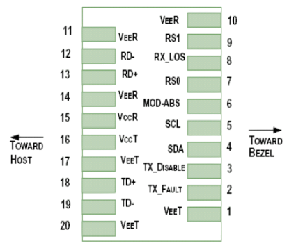
Figure1. Diagram of host board connector block pin numbers and names
|
PIN |
Name |
Name/Description |
Notes |
|
1 |
VeeT |
Transmitter Ground |
1 |
|
2 |
TX_Fault |
Transmitter Fault |
|
|
3 |
TX_Disable |
Transmitter Disable; Turns off transmitter laser output |
|
|
4 |
SDA |
Two wire serial interface Data Line (LVCMOS-I/O) (MOD-DEF2) |
2 |
|
5 |
SCL |
Two wire serial interface Clock Line (LVCMOS-I/O) (MOD-DEF1) |
2 |
|
6 |
MOD_ABS |
Module Definition, Grounded in the module |
|
|
7 |
RS0 |
Rx Rate Select: |
|
|
8 |
RX_LOS |
Receiver Loss of Signal Indication Active LOW |
|
|
9 |
RS1 |
Transmitter Rate Select (not used) |
|
|
10 |
VeeR |
Receiver Ground |
1 |
|
11 |
VeeR |
Receiver Ground |
1 |
|
12 |
RD- |
Receiver Inverted Data Output |
|
|
13 |
RD+ |
Receiver Data Output |
|
|
14 |
VeeR |
Receiver Ground |
1 |
|
15 |
VccR |
Receiver Power - +3.3V |
|
|
16 |
VccT |
Transmitter Power - +3.3 V |
|
|
17 |
VeeT |
Transmitter Ground |
1 |
|
18 |
TD+ |
Transmitter Non-Inverted Data Input |
|
|
19 |
TD- |
Transmitter Inverted Data Input |
|
|
20 |
VeeT |
Transmitter Ground |
1 |
Notes:
1. Module ground pins GND are isolated from the module case.
2. Shall be pulled up with 4.7K-10Kohms to a voltage between 3.15V and 3.47V on the host board.
Electrical Characteristics
The following electrical characteristics are defined over the Recommended Operating Environment unless otherwise specified.
|
Parameter |
Symbol |
Min. |
Typ. |
Max |
Unit |
Notes |
|
Power Consumption |
p |
1.0 |
W |
|||
|
Supply Current |
Icc |
300 |
mA |
|||
|
Transmitter |
||||||
|
Single-ended Input Voltage Tolerance |
Vcc |
-0.3 |
4.0 |
V |
||
|
common mode voltage tolerance |
15 |
mV |
||||
|
Differential Input Voltage Swing |
Vin,pp |
180 |
700 |
mVp p |
||
|
Differential Input Impedance |
Zin |
90 |
100 |
110 |
Ohm |
1 |
|
Transmit Disable Assert Time |
10 |
us |
||||
|
Transmit Disable Voltage |
Vdis |
Vcc-1.3 |
Vcc |
V |
||
|
Transmit Enable Voltage |
Ven |
Vee |
Vee +0.8 |
V |
2 |
|
|
Receiver |
||||||
|
Single-ended Input Voltage Tolerance |
Vcc |
-0.3 |
4.0 |
V |
||
|
Differential Output Voltage Swing |
Vout,pp |
300 |
900 |
mVp p |
||
|
Differential Output Impedance |
Zout |
90 |
100 |
110 |
Ohm |
3 |
|
Data output rise/fall time |
Tr/Tf |
9.5 |
ps |
4 |
||
|
LOS Assert Voltage |
VlosH |
Vcc-1.3 |
Vcc |
V |
5 |
|
|
LOS De-assert Voltage |
VlosL |
Vee |
Vee +0.8 |
V |
5 |
|
Notes:
- Or open circuit.
- These are unfiltered 20-80% values.
- Input 100 ohms differential termination.
- Connected directly to TX data input pins. AC coupled thereafter.
- Loss of Signal is LVTTL. Logic 0 indicates normal operation; logic 1 indicates no signal detected.
Optical Characteristics
The following optical characteristics are defined over the Recommended Operating Environment unless otherwise specified.
|
Parameter |
Symbol |
Min. |
Typical |
Max |
Unit |
Notes |
|
Transmitter |
||||||
|
Center Wavelength |
λC |
840 |
850 |
860 |
nm |
|
|
Optical Spectral Width |
∆λ |
0.6 |
nm |
|||
|
Average Optical Power |
PAVG |
-8.4 |
2.4 |
dBm |
1 |
|
|
Optical Extinction Ratio |
ER |
2.0 |
dB |
2 |
||
|
Transmitter OFF Output Power |
Poff |
-30 |
dBm |
|||
|
Transmitter and Dispersion Penalty |
TDP |
4.4 |
dB |
|||
|
Optical Return Loss Tolerance |
ORLT |
12 |
dB |
|||
|
Transmitter Eye Mask |
Compliant with IEEE802.3ae |
|||||
|
Receiver |
||||||
|
Center Wavelength |
λC |
840 |
850 |
860 |
nm |
|
|
Receiver Sensitivity in average power @10.3125Gbps |
Sen. |
-10 |
dBm |
3 |
||
|
Receiver Sensitivity in average power @25.78125Gbps |
Sen. |
-10.3 |
dBm |
4 |
||
|
Stressed Sensitivity (OMA) |
-5.2 |
dBm |
4 |
|||
|
Input Saturation Power (OMA) |
Psat |
3 |
dBm |
|||
|
LOS Assert |
LOSA |
-20 |
dBm |
|||
|
LOS De-assert |
LOSD |
-11 |
dBm |
|||
|
Optical Return Loss |
ORL |
12 |
dB |
|||
|
LOS Hysteresis |
LOSH |
0.5 |
dB |
|||
Notes:
- Class 1 Laser Safety per FDA/CDRH and IEC-825-1 regulations.
- λc refer to wavelength selection, and corresponds to approximately 0.8 nm.
-
Measured with Light source 1528.77~1563.86nm, ER=6dB; BER =<10^-12 @ PRBS=2^31-1 NRZ.
Digital Diagnostic Functions
The following digital diagnostic characteristics are defined over the Recommended Operating Environment unless otherwise specified. It is compliant to SFF-8472 Rev10.2 with internal calibration mode. For external calibration mode please contact our sales staff.
|
Parameter |
Symbol |
Min. |
Max |
Unit |
Notes |
|
Temperature monitor absolute error |
DMI_ Temp |
-3 |
3 |
℃ |
Over operating temp |
|
Supply voltage monitor absolute error |
DMI _VCC |
-3 |
3 |
% |
Full operating range |
|
RX power monitor absolute error |
DMI_RX |
-3 |
3 |
dB |
|
|
Bias current monitor |
DMI_ bias |
-10 |
10 |
% |
|
|
TX power monitor absolute error |
DMI_TX |
-3 |
3 |
dB |
Mechanical Dimensions
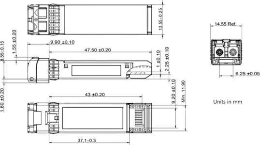
Figure2. Mechanical Outline
If you need more support , Please contact us .
