

Click to open expanded view
100G QSFP28 2km Optical Transceiver
Features
l Lane bit rate 25.78 Gb/s;
l Single +3.3V power supply;
l Compliant to IEEE802.3bm;
l Up to 2km transmission on SMF;
l Compliant to 100G CWDM4 MSA;
l CWDM DML laser and PIN receiver;
l Maximum power consumption 3.5 W;
l Compliant to SFF-8665 and SFF-8679;
l Operating case temperature: 0 to +70 °C;
l High speed I/O electrical interface (CAUI-4);
l Supports 100GBASE-CWDM4(103.1Gb/s);
l Complies with EU Directive 2011/65/EU (RoHS 6);
l QSFP28 MSA package with duplex LC connector;
l I2C interface with integrated Digital Diagnostic monitoring;
Application
l 100GBASE-CWDM4 application with FEC;
Absolute Maximum Ratings
Table 1-Absolute Maximum Ratings
|
Parameter |
Symbol |
Min. |
Typical |
Max. |
Unit |
Notes |
|
Storage Temperature |
TS |
-40 |
- |
+85 |
°C |
|
|
Supply Voltage |
VCC |
-0.5 |
- |
+4.0 |
V |
|
|
Operating Relative Humidity |
RH |
- |
- |
+85 |
% |
|
Recommended Operating Conditions
Table 2-Recommended Operating Conditions
|
Parameter |
Symbol |
Min. |
Typical |
Max. |
Unit |
Notes |
|
Operating Case Temperature |
TC |
0 |
- |
+70 |
°C |
|
|
Power Supply Voltage |
VCC |
3.13 |
3.3 |
3.47 |
V |
|
|
Power Supply Current |
ICC |
- |
- |
1.1 |
A |
|
|
Maximum Power Dissipation |
PD |
- |
- |
3.5 |
W |
|
|
Aggregate Bit Rate |
BRAVE |
- |
103.125 |
- |
Gb/s |
|
|
Lane Bit Rate |
BRLANE |
- |
25.78 |
- |
Gb/s |
|
|
Transmission Distance |
TD |
|
- |
2 |
km |
Over SMF |
Optical Characteristics
Table 3-Optical Characteristics
|
Transmitter |
||||||
|
Parameter |
Symbol |
Min. |
Typical |
Max. |
Unit |
Notes |
|
Center Wavelength Lane 0 |
λ0 |
1264.5 |
1271 |
1277.5 |
nm |
|
|
Center Wavelength Lane 1 |
λ1 |
1284.5 |
1291 |
1297.5 |
nm |
|
|
Center Wavelength Lane 2 |
λ2 |
1304.5 |
1311 |
1317.5 |
nm |
|
|
Center Wavelength Lane 3 |
λ3 |
1324.5 |
1331 |
1337.5 |
nm |
|
|
Total Launch Power, 100GE |
PALL |
- |
- |
8.5 |
dBm |
1 |
|
Average Launch Power per Lane, 100GE |
PTX_LANE |
-6.5 |
- |
2.5 |
dBm |
1 |
|
OMA per Lane, 100GE |
OMA |
-4 |
- |
2.5 |
dBm |
1 |
|
OMA–TDP per Lane, 100GE |
OMA_TDP |
-5.0 |
- |
- |
dBm |
|
|
Difference in launch power between lanes |
PTX_Delta_LANE |
- |
- |
6.0 |
dB |
|
|
Average Output Power (Laser Turn off) |
P0UT-OFF |
- |
- |
-30 |
dBm |
|
|
Side Mode Suppression Ratio |
SMSR |
30 |
- |
- |
dB |
|
|
Extinction Ratio, 100GE |
ER |
3.5 |
- |
- |
dB |
|
|
Transmitter and Dispersion Penalty |
TDP |
- |
- |
3.0 |
dB |
2 |
|
Optical Return Loss Tolerance |
ORLT |
- |
- |
20 |
dB |
|
|
Optical Eye Mask, 100GE {X1,X2,X3,Y1,Y2,Y3} |
Compliant with 100G CWDM4 MSA {0.31,0.4,0.45,0.34,0.38,0.4} |
2 |
||||
|
Receiver |
||||||
|
Parameter |
Symbol |
Min. |
Typical |
Max. |
Unit |
Notes |
|
Center Wavelength Lane 0 |
λ0 |
1264.5 |
1271.0 |
1277.5 |
nm |
|
|
Center Wavelength Lane 1 |
λ1 |
1284.5 |
1291.0 |
1297.5 |
nm |
|
|
Center Wavelength Lane 2 |
λ2 |
1304.5 |
1311.0 |
1317.5 |
nm |
|
|
Center Wavelength Lane 3 |
λ3 |
1324.5 |
1331.0 |
1337.5 |
nm |
|
|
OMA Sensitivity per Lane, 100GE |
Rxsens |
- |
- |
-11.5 |
dBm |
3 |
|
Stressed receiver sensitivity (OMA), perlane |
SRS_OMA |
- |
- |
-7.3 |
dBm |
3 |
|
SRS eye mask definition, 100GE {X1,X2,X3,Y1,Y2,Y3} |
Compliant with 100G CWDM4 MSA {0.39,0.5,0.5,0.39,0.39,0.4} |
|
||||
|
Damage threshold |
Pdamage |
3.5 |
- |
- |
dBm |
|
|
Receive Saturation (OMA) per Lane |
Rmax |
2.5 |
- |
- |
dBm |
|
|
Reflectance |
Ref |
- |
- |
-26 |
dB |
|
|
LOS Assert per lane |
LOSA |
-25 |
- |
- |
dBm |
|
|
LOS De-assert |
LOSD |
- |
- |
-13 |
dBm |
|
|
LOS Hysteresis |
LOSH |
0.5 |
- |
6 |
dB |
|
1. The optical power is launched into SMF.
2. Measured with a PRBS 231-1 test pattern @25.78125Gb/s, Hit ratio≤5E-5.
3. Measured with a PRBS 231-1 test pattern @25.78125 Gb/s, BER≤5E-5.
Electrical Characteristics
High-Speed Signal: Compliant to CAUI-4 (IEEE 802.3bm)
Low-Speed Signal: Compliant to QSFP-8679.
Table 4-Electrical Characteristics
|
Transmitter (Module Input) |
||||||
|
Parameter |
Symbol |
Min. |
Typical |
Max. |
Unit |
Notes |
|
Differential Data Input Amplitude |
VIN,P-P |
85 |
- |
900 |
mVpp |
|
|
Differential Termination Mismatch |
|
- |
- |
10 |
% |
|
|
LPMode, Reset and ModSelL, V in low |
VIL |
-0.3 |
- |
0.8 |
V |
|
|
LPMode, Reset and ModSelL, V in high |
VIH |
2.0 |
- |
VCC+0.3 |
V |
|
|
Receiver (Module Output) |
||||||
|
Parameter |
Symbol |
Min. |
Typical |
Max. |
Unit |
Notes |
|
Differential Data Output Amplitude |
VOUT,P-P |
200 |
- |
900 |
mVpp |
|
|
Differential Termination Mismatch(1MHZ) |
|
- |
- |
10 |
% |
|
|
Output Rise/Fall Time, 20%~80% |
TR |
12 |
- |
- |
ps |
|
|
ModPrsL and IntL, V out low |
VOL |
0 |
- |
0.4 |
V |
|
|
ModPrsL and IntL, V out high |
VOH |
VCC-0.5 |
- |
VCC+0.3 |
V |
|
Digital Diagnostics
Table 5-Digital Diagnostics
|
Parameter |
Range |
Accuracy |
Unit |
Calibration |
|
Temperature |
0 to 70 |
±3 |
ºC |
Internal |
|
Voltage |
0 to VCC |
0.1 |
V |
Internal |
|
Tx Bias Current Per Lane |
0 to 100 |
10% |
mA |
Internal |
|
Tx Output Power Per Lane |
-6.5 to 3 |
±3 |
dBm |
Internal |
|
Rx Power (Each Lane) |
-11.5 to 3 |
±3 |
dBm |
Internal |
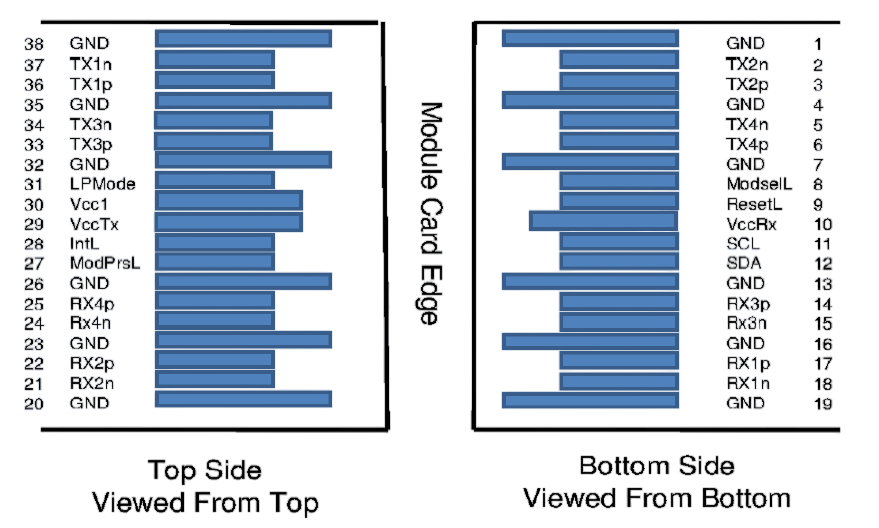
Pin Definitions
|
PIN |
Logic |
Symbol |
Description |
Plug |
Notes |
|
1 |
|
GND |
Ground |
1 |
1 |
|
2 |
CML-I |
Tx2n |
Transmitter Inverted Data Input |
3 |
|
|
3 |
CML-I |
Tx2p |
Transmitter Non-Inverted Data output |
3 |
|
|
4 |
|
GND |
Ground |
1 |
1 |
|
5 |
CML-I |
Tx4n |
Transmitter Inverted Data Input |
3 |
|
|
6 |
CML-I |
Tx4p |
Transmitter Non-Inverted Data output |
3 |
|
|
7 |
|
GND |
Ground |
1 |
1 |
|
8 |
LVTLL-I |
ModSelL |
Module Select |
3 |
|
|
9 |
LVTLL-I |
ResetL |
Module Reset |
3 |
|
|
10 |
|
VccRx |
﹢3.3V Power Supply Receiver |
2 |
2 |
|
11 |
LVCMOS-I/O |
SCL |
2-Wire Serial Interface Clock |
3 |
|
|
12 |
LVCMOS-I/O |
SDA |
2-Wire Serial Interface Data |
3 |
|
|
13 |
|
GND |
Ground |
1 |
|
|
14 |
CML-O |
Rx3p |
Receiver Non-Inverted Data Output |
3 |
|
|
15 |
CML-O |
Rx3n |
Receiver Inverted Data Output |
3 |
|
|
16 |
|
GND |
Ground |
1 |
1 |
|
17 |
CML-O |
Rx1p |
Receiver Non-Inverted Data Output |
3 |
|
|
18 |
CML-O |
Rx1n |
Receiver Inverted Data Output |
3 |
|
|
19 |
|
GND |
Ground |
1 |
1 |
|
20 |
|
GND |
Ground |
1 |
1 |
|
21 |
CML-O |
Rx2n |
Receiver Inverted Data Output |
3 |
|
|
22 |
CML-O |
Rx2p |
Receiver Non-Inverted Data Output |
3 |
|
|
23 |
|
GND |
Ground |
1 |
1 |
|
24 |
CML-O |
Rx4n |
Receiver Inverted Data Output |
3 |
|
|
25 |
CML-O |
Rx4p |
Receiver Non-Inverted Data Output |
3 |
|
|
26 |
|
GND |
Ground |
1 |
1 |
|
27 |
LVTTL-O |
ModPrsL |
Module Present |
3 |
|
|
28 |
LVTTL-O |
IntL |
Interrupt |
3 |
|
|
29 |
|
VccTx |
+3.3 V Power Supply transmitter |
2 |
2 |
|
30 |
|
Vcc1 |
+3.3 V Power Supply |
2 |
2 |
|
31 |
LVTTL-I |
LPMode |
Low Power Mode |
3 |
|
|
32 |
|
GND |
Ground |
1 |
1 |
|
33 |
CML-I |
Tx3p |
Transmitter Non-Inverted Data Input |
3 |
|
|
34 |
CML-I |
Tx3n |
Transmitter Inverted Data Output |
3 |
|
|
35 |
|
GND |
Ground |
1 |
1 |
|
36 |
CML-I |
Tx1p |
Transmitter Non-Inverted Data Input |
3 |
|
|
37 |
CML-I |
Tx1n |
Transmitter Inverted Data Output |
3 |
|
|
38 |
|
GND |
Ground |
1 |
1 |
|
Note 1: GND is the symbol for signal and supply (power) common for the QSFP28 module. All are common within the QSFP28 module and all module voltages are referenced to this potential unless otherwise noted. Connect these directly to the host board signal-common ground plane. |
|||||
|
Note 2: Vcc Rx, Vcc1 and Vcc Tx are the receiver and transmitter power supplies and shall be applied concurrently. Requirements defined for the host side of the Host Edge Card Connector are listed in MSA. The connector pins are each rated for a maximum current of 1000 mA. |
|||||
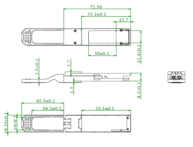
Mechanical Dimension
Ordering Information
|
Part No. |
Data Rate |
Laser |
Fiber Type |
Distance |
Optical Interface |
Temp |
DDMI |
|
HC-Q28-C31L-2D |
103.1Gbps |
CWDM DML |
SMF |
2km |
LC |
0~70C |
Y |
If you need more support , Please contact us .
