


Thin film lithium niobate phase modulator
Product description
Thin film lithium niobate phase modulator is a high-performance electro-optic conversion device, which is independently developed by our company and has complete independent intellectual property rights. The product is packaged by high-precision coupling process technology to achieve ultra-high electro-optical conversion efficiency. Compare with that traditional lithium niobate modulator, the product has the characteristics of low half-wave voltage, high stability and small device size, and can be widely apply to the fields of digital optical communication, microwave photonics, backbone communication networks, communication scientific research projects and the like.
Product features
RF bandwidth up to 40 GHz
Half-wave voltage down to 3 V
Insertion loss as low as 4.5 dB
Small device size
Technical parameters
|
Category |
Parameter |
Symbol |
Unit |
Indicators |
|
|
Optical Performance (@ 25 ° C) |
Operating Wavelength (*) |
λ |
nm |
~1550 |
|
|
Optical return loss |
ORL |
dB |
≤ -27 |
||
|
Optical insertion loss (*) |
IL |
dB |
Maximum: 5.5 Typical value: 4.5 |
||
|
Electrical properties (@25°C) |
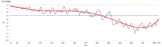
3 dB electro-optic bandwidth (From 2 GHz) |
S21 |
GHz |
X1: 2 |
X1: 4 |
|
Minimum: 18 Typical value: 20 |
Minimum: 36 Typical value: 40 |
||||
|
RF half-wave voltage (@ 50 kHz) |
Vπ |
V |
Maximum: 3.5 Typical value: 3.0 |
||
|
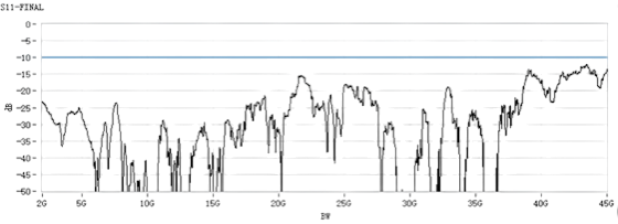
RF return loss (2 to 40 GHz) |
S11 |
dB |
≤ -10 |
||
|
Working conditions |
Operating temperature |
TO |
°C |
-20~70 |
|
* Customizable.
Damage threshold
If the device works beyond the maximum damage threshold, it will cause irreversible damage to the device, and such device damage is not within the scope of maintenance service.
|
Parameter |
Symbol |
Optional |
Minimum value |
Maximum value |
Unit |
|
RF input power |
Sin |
X2: 4 |
- |
18 |
dBm |
|
X2: 5 |
- |
29 |
|||
|
RF Input Swing Voltage |
Vpp |
X2: 4 |
-2.5 |
+2.5 |
V |
|
X2: 5 |
-8.9 |
+8.9 |
|||
|
RF Input RMS Voltage |
Vrms |
X2: 4 |
- |
1.78 |
V |
|
X2: 5 |
- |
6.30 |
|||
|
Optical input power |
Pin |
- |
- |
20 |
dBm |
|
Storage temperature |
Ts |
- |
-40 |
85 |
℃ |
|
Relative humidity (no condensation) |
RH |
- |
5 |
90 |
% |
Package dimensions and pin definitions (mm)
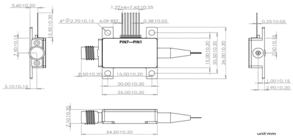
Note: Data marked with REF. Are reference values only.
|
Pin |
Symbol |
Description |
|
1 |
- |
No definition |
|
2 |
- |
No definition |
|
3 |
- |
No definition |
|
4 |
- |
No definition |
|
5 |
- |
No definition |
|
6 |
- |
No definition |
|
7 |
- |
No definition |
|
RF |
RF Connector (*) |
2.92 mm K connector |
|
In |
Incoming optical fiber |
FC/APC, PMF |
|
Out |
Light-emitting fiber |
FC/APC, PMF |
* Customizable 1.85 mm connector or J connector.
S21 Test Sample (40 GHz Typical)
Ordering information
HC- LB-X1C6PPBP6X2
|
Optional |
Description |
Option number |
|
X1 |
3 dB electro-optic bandwidth |
2 : 20G 4: 40G |
|
X2 |
Maximum RF input power |
4 or 5 |
Product description: 20 GHz/40 GHz thin-film lithium niobate phase modulator.
If you need more information , Please contact us .
