

Click to open expanded view
100Gbps QSFP28 BIDI Transceiver, 40KM Reach
Product Features
Ø QSFP28 MSA package with simplex LC connector
Ø Compliant to 100G Lamda MSA 100G-ER1 Optical Specifications
Ø Two Wire Serial Interface with Digital Diagnostic Monitoring
Ø Support KP4 FEC inside the module and KP4 FEC shutdown
Ø Lane signaling rate 53.125GBd with PAM4
Ø High speed I/O electrical interface
Ø Maximum power consumption 4.5W
Ø Reaches up to 40km on SMF
Ø 3.3V power supply voltage
Ø Compliant to RoHS2.0
Ø Class 1 Laser
Ø Operating case temperature range :
commercial grade: 0~+70℃ , industrial grade: - 40 ~85℃
Applications
Ø Switch/Router
Ø 100G BASE Ethernet
Ø Data center network networking
Description
This transceiver provides 100GBase-BX throughput up to 40km over single-mode fiber (SMF).Use center wavelength 1304nm/1309nm through LC connector.This bidirectional unit must be used with another transceiver or network appliance of complimenting wavelengths. Digital diagnostics functions are also available via the I2C interface, as specified by the QSFP28 MSA, to allow access to real-time operating parameters. With these features, this easy to install, hot swappable transceiver is suitable to be used in various applications, such as 100G Ethernet, data center, and storage area networks applications.
Absolute Maximum Ratings
It has to be noted that the operation in excess of any individual absolute maximum ratings might cause permanent damage to this module.
Table 1 -Absolute Maximum Ratings
|
Parameter |
Symbol |
Min |
Max |
Unit |
Note |
|
Storage Temperature |
TS |
-40 |
85 |
°C |
|
|
Operating Case Temperature |
TOP |
0 |
70 |
°C |
|
|
Power Supply Voltage |
VCC |
-0.5 |
4 |
V |
|
|
Relative Humidity (non-condensation) |
RH |
0 |
85 |
% |
|
Recommended Operating Conditions
Table 2 -Recommended Operating Conditions
|
Parameter |
Symbol |
Min |
Typical |
Max |
Unit |
Note |
|
Operating Case Temperature |
TOP |
0 |
|
70 |
°C |
|
|
Power Supply Voltage |
VCC |
3.135 |
3.3 |
3.465 |
V |
|
|
Power Consumption |
|
|
|
4.5 |
W |
|
|
Supply Current |
Icc |
|
|
1.3 |
A |
|
|
Aggregate Bit Rate |
BRAVE |
- |
103.125 |
106.25 |
Gb/s |
|
|
Lane Bit Rate |
BRLANE |
- |
25.78 |
26.5625 |
Gb/s |
|
|
Transmission Distance |
TD |
|
|
40 |
KM |
Over SMF |
Optical Characteristics
Table 3 -Optical Characteristics
|
Parameter |
Symbol |
Condition |
Min. |
Typ. |
Max. |
Unit |
Note |
|
Transmitter |
|||||||
|
Data Rate |
|
|
|
103.125 |
106.25 |
Gbps |
|
|
Data rate variation |
|
|
-100 |
|
+100 |
ppm |
|
|
Lane center wavelength |
|
|
1304.06 |
1304.58 |
1305.1 |
nm |
|
|
1308.61 |
1309.14 |
1309.66 |
nm |
|
|||
|
Launch power |
Peach |
|
1.5 |
|
7.1 |
dBm |
1,2 |
|
Optical modulation amplitude |
POMA |
For TDECQ <1.4dB
|
4.5 |
|
7.9 |
dBm |
|
|
For 1.4dB< TDECQ
Q(max)
|
3.1+ TDEC Q |
|
7.9 |
|
|
||
|
Transmitter and Dispersion eye closure |
TDECQ |
|
|
|
3.9 |
dBm |
|
|
Optical Extinction Ratio |
ER |
|
6 |
|
|
dB |
|
|
Side mode Suppression ratio |
SMSR |
|
30 |
|
|
dB |
|
|
Launch power of OFF Transmitter |
|
|
|
|
-30 |
dBm |
|
|
Relative Intensity Noise |
RIN |
|
|
|
-136 |
dB/Hz |
|
|
Optical return loss tolerance |
|
|
|
|
15.6 |
dB |
|
|
Transmitter reflectance |
|
|
|
|
-26 |
dB |
4 |
|
Receiver |
|||||||
|
Data Rate |
|
|
|
103.125 |
106.25 |
Gbps |
|
|
Data rate variation |
|
|
-100 |
|
+100 |
ppm |
|
|
Lane center wavelength |
|
|
1308.61 |
1309.14 |
1309.66 |
nm |
|
|
|
|
1304.06 |
1304.58 |
1305.1 |
nm |
|
|
|
Damage threshold |
Rdam |
|
-2.4 |
|
|
dBm |
5 |
|
Average receiver power |
Rpow |
|
-16.2 |
|
-3.4 |
dBm |
6 |
|
Receiver power(OMA) |
Rovl |
|
|
|
-2.6 |
dBm |
|
|
Receiver sensitivity (OMA), (max) |
SOMA |
For TDECQ <1.4dB |
|
|
-14.0 |
dBm |
@BER2.4e-4
|
|
For 1.4dB< TDECQ <3.9 |
|
|
-15.4+ TECQ |
dBm |
|||
|
Stressed Sensitivity |
SRS |
|
|
|
-11.5 |
dBm |
8 |
|
Receiver reflectance |
|
|
|
|
-26 |
dB |
|
|
LOSS assert |
Optical power alarm |
|
-26 |
|
-18 |
dBm |
|
|
LOSS de-assert |
|
|
|
|
-16 |
dBm |
|
|
Conditions of stressed receiver sensitivity test: |
|||||||
|
Stressed eye closure for PAM4 (SECQ), |
|
|
|
|
3.9 |
dB |
8 |
Notes:
1、As the total average launch power limit has to be met, not all of the lanes can operate at the maximum average launch power ,each lane.
2、Average launch power, each lane(min) is informative and not the principal indicator of signal strength. A transmitter with launch power below this value can not be compliant: however, a value above this does not ensure compliance.
3、Transmitter reflectance is defined looking into the transmitter.
4、The receiver shall be able to tolerate, without damage, continuous exposure to an optical input signal having this average power level.
5、Average receiver power, each lane(min) is informative and not the principal indicator of signal strength. A received power below this value cannot be compliant; however, a value above this does not ensure compliance.
6、Measured with conformance test signal at TP3 for the BER specified in 《100G-FR and 100G-LR1 Technical Specifications Rev 2.0》
7、These test conditions are for measuring stressed receiver sensitivity. They are not characteristics of the receiver.
Electrical Characteristics
The following electrical characteristics are defined over the recommended operating environment
Table 4 -Electrical Characteristics
|
Transmitter (Module Input) |
||||||
|
Parameter |
Symbol |
Min. |
Typical |
Max. |
Unit |
Notes |
|
Input Differential Impedance |
Rin |
- |
100 |
- |
Ohm |
|
|
Differential Data Input Amplitude |
VIN,P-P |
80 |
- |
900 |
mVpp |
|
|
Differential termination mismatch (max) |
D-mismatch |
- |
- |
10 |
% |
|
|
DC common-mode input voltage |
|
-0.3 |
- |
2.8 |
V |
|
|
Transition time(20%~80%) |
Tr Tf |
10 |
- |
- |
ps |
|
|
LPMode, Reset and ModSelL / Tx dis |
VIL |
-0.3 |
- |
0.8 |
V |
|
|
LPMode, Reset and ModSelL / Tx dis |
VIH |
2.0 |
- |
VCC+0.3 |
V |
|
|
Receiver (Module Output) |
||||||
|
Output Differential Impedance |
Rout |
- |
100 |
- |
Ohm |
|
|
Differential Data Output Amplitude |
VOUT,P-P |
- |
- |
900 |
mVpp |
|
|
Differential termination mismatch (max) |
D-mismatch |
- |
- |
10 |
% |
|
|
Transition time, 20% to 80% |
Tr Tf |
12 |
- |
|
ps |
|
|
ModPrsL and IntL/ Rx los |
VOL |
0 |
- |
0.4 |
V |
|
|
ModPrsL and IntL/ Rx los |
VOH |
VCC-0.5 |
- |
VCC+0.3 |
V |
|
Digital Diagnostics
Table 6-Digital Diagnostics
|
Parameter |
Symbol |
Min |
Max |
Unit |
Note |
|
Temperature Monitor Absolute Error |
DMI_Temp |
-3 |
3 |
°C |
Cover full operating temperature range |
|
Supply Voltage Monitor Absolute Error |
DMI _VCC |
-0.1 |
0.1 |
V |
Cover full operating temperature range |
|
Channel RX Power Monitor Absolute Error |
DMI_RX_Ch |
-3 |
3 |
dB |
|
|
Channel Bias Current Monitor |
DMI_Ibias_Ch |
-10% |
10% |
|
|
|
Channel TX Power Monitor Absolute Error |
DMI_TX_Ch |
-3 |
3 |
dB |
|
Edge connector and pinout description
The electrical pinout of the QSFP28 module is shown in Figure 1 below.
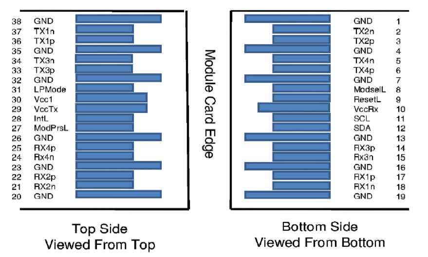
|
PIN |
Symbol |
Name/Description |
Note |
|
1 |
GND |
Ground |
1 |
|
2 |
Tx2n |
Transmitter Inverted Data Input |
|
|
3 |
Tx2p |
Transmitter Non-Inverted Data output |
|
|
4 |
GND |
Ground |
1 |
|
5 |
Tx4n |
Transmitter Inverted Data Input |
|
|
6 |
Tx4p |
Transmitter Non-Inverted Data output |
|
|
7 |
GND |
Ground |
1 |
|
8 |
ModSelL |
Module Select |
3 |
|
9 |
ResetL |
Module Reset |
4 |
|
10 |
VccRx |
+3.3V Power Supply Receiver |
2 |
|
11 |
SCL |
2-Wire Serial Interface Clock |
3 |
|
12 |
SDA |
2-Wire Serial Interface Data |
3 |
|
13 |
GND |
Ground |
1 |
|
14 |
Rx3p |
Receiver Non-Inverted Data Output |
|
|
15 |
Rx3n |
Receiver Inverted Data Output |
|
|
16 |
GND |
Ground |
1 |
|
17 |
Rx1p |
Receiver Non-Inverted Data Output |
|
|
18 |
Rx1n |
Receiver Inverted Data Output |
|
|
19 |
GND |
Ground |
1 |
|
20 |
GND |
Ground |
1 |
|
21 |
Rx2n |
Receiver Inverted Data Output |
|
|
22 |
Rx2p |
Receiver Non-Inverted Data Output |
|
|
23 |
GND |
Ground |
1 |
|
24 |
Rx4n |
Receiver Inverted Data Output |
|
|
25 |
Rx4p |
Receiver Non-Inverted Data Output |
|
|
26 |
GND |
Ground |
1 |
|
27 |
ModPrsL |
Module Present |
|
|
28 |
IntL |
Interrupt |
5 |
|
29 |
VccTx |
+3.3 V Power Supply transmitter |
2 |
|
30 |
Vcc1 |
+3.3 V Power Supply |
2 |
|
31 |
LPMode |
Low Power Mode |
5 |
|
32 |
GND |
Ground |
1 |
|
33 |
Tx3p |
Transmitter Non-Inverted Data output |
|
|
34 |
Tx3n |
Transmitter Inverted Data Input |
|
|
35 |
GND |
Ground |
1 |
|
36 |
Tx1p |
Transmitter Non-Inverted Data output |
|
|
37 |
Tx1n |
Transmitter Inverted Data Input |
|
|
38 |
GND |
Ground |
1
|
Notes:
1. GND is the symbol for signal and supply (power) common for QSFP28 modules. All are common within the QSFP28 module and all module voltages are referenced to this potential.unless otherwise noted. Connect these directly to the host board signal common ground plane.
2. Vcc Rx, Vcc1 and Vcc Tx are the receiver and transmitter power suppliers and shall be applied concurrently. Vcc Rx, Vcc1 and Vcc Tx may be internally connected within the QSFP28 transceiver module in any combination. The connector pins are each rated for a maximum current of 1000mA.
3. Timing for SCL, SDA and ModSelL shall comply with the common management interface document SFF-8636 and SFF-8679.
4. The QSFP28 module must support hardware reset operation.
5. Two Multi-Purpose PIN for supporting Tx_DIS and Rx_LOS function in the 100G QSFP28 module.The IIC interface must function normally when the QSFP28 module is in the LP mode.
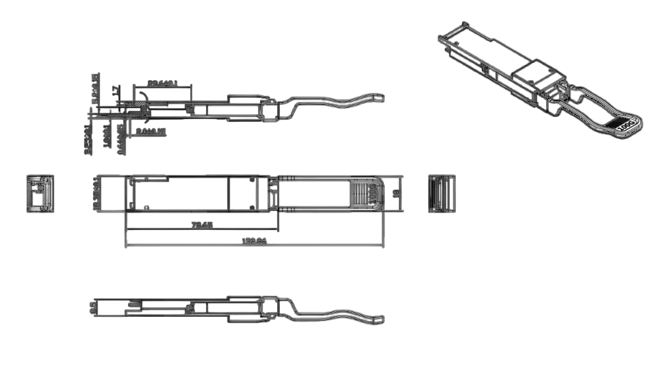
Mechanical Dimension
Order Information
|
Part No. |
Data Rate |
Laser |
Fiber Type |
Distance |
Optical Interface |
DDM |
|
HC-Q28-B49L-40D/ HC-Q28-B94L-40D |
106.25Gbps |
EML |
SMF |
40KM |
Simplex LC |
Y |
|
Temp |
Commercial grade: 0~+70℃ ,Industrial grade: - 40 ~85℃ |
|||||
If you need more support , Please contact us.
