
Click to open expanded view
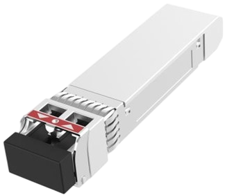
10G BIDI SFP+ TX1330nm RX 1270nm 40km LC Transceiver
Features
Hot pluggable
+3.3V power supply
Up to 10.3125Gbps
Up to 40 km transmission on SMF
1330nm DFB laser and PIN receiver
Power consumption less than 1.0W
Operating case temperature:0~+70℃
Very low EMI and excellent ESD protection
SFP+MSA package with single LC connector
Electronic Interface compliant with SFF-8431
2-wire interface for integrated Digital Diagnosticmonitoring
Applications
Custom high-speed data pipes
Computer cluster cross-connect
High-speed storage area networks
Description
This transceiver is a high performance,cost effective modules,which is supporting up to10.3125Gbps,and transmission distance up to 40km on SM fiber.The transceiver consists of two sections:The transmitter section incorporates a laser driver and a1330nm DFB laser.The receiver section consists ofaPIN photodiode integrated with a transimpedance preamplifier(TIA)and a Limitting Amplifier.The moduleis hot pluggable into the 20-pin connector.The high-speed electrical interface is base on low voltage logic,with nominal100Ohms differential impedance and AC coupled in the module.
The optical output can be disabled by LVTTLlogic high-level input ofTX_DIS.Transmit Fault(Tx_Fault)isprovided to indicate that the module transmitter has detected a fault condition related to laser operation orsafety.Loss of signal(RX_LOS)output is provided to indicate the loss of an input optical signal ofreceiver.Aserial EEPROM in the transceiver allows the user to access transceiver monitoring and configuration data viathe 2-wire SFPManagement Interface.This interface uses a single address,A0h,with a memory map dividedinto a lower and upper area.Basic digital diagnostic(DD)data is held in the lower area while specific data isheld in a series of tables in the high memory area.
Technical Specification
|
Absolute Maximum Ratings |
|||||
|
Parameter |
Symbol |
Min. |
Max. |
Unit |
Notes |
|
Storage Temperature |
TS |
-40 |
+85 |
℃ |
|
|
Supply Voltage |
VCC3 |
0 |
3.6 |
V |
|
|
Relative Humidity |
RH |
5 |
+85 |
% |
Note1 |
|
Rx Input Average Power |
Pmax |
- |
+1.5 |
dBm |
|
Notes:
[1] Non-condensing state.
|
Recommended Operating Conditions |
|||||
|
Parameter |
Symbol |
Min. |
Typical |
Max. |
Unit |
|
Operating Case Temperature |
TC |
0 |
25 |
+70 |
℃ |
|
Power Supply Voltage |
VCC3 |
3.13 |
3.3 |
3.47 |
V |
|
ICC3 |
- |
- |
300 |
mA |
|
|
Power Dissipation |
PD |
- |
- |
1.0 |
W |
|
Data Rate |
|
|
10.3125 |
|
Gbps |
|
Transmission Distance |
- |
- |
10 |
Km |
|
|
Transmitter Operating Characteristic-Optical, Electrical |
||||||
|
Parameter |
Symbol |
Min. |
Typical |
Max. |
Unit |
Note |
|
Centre Wavelength |
λC |
1310 |
1330 |
1350 |
nm |
|
|
Spectral Width |
Δλ |
|
|
1 |
nm |
DFB |
|
Side Mode Suppression Ratio |
SMSR |
30 |
- |
- |
dB |
|
|
Laser Off Power |
Poff |
- |
- |
-30 |
dBm |
|
|
Average Optical Power |
Pavg |
1 |
- |
5 |
dBm |
|
|
Extinction Ratio |
ER |
3.5 |
- |
- |
dB |
|
|
Transmitter Dispersion Penalty |
TDP |
- |
- |
3.2 |
dB |
|
|
Relative Intensity Noise |
RIN12OMA |
- |
- |
-128 |
dB/Hz |
|
|
Optical Return Loss Tolerance |
ORLT |
- |
- |
12 |
dB |
|
|
Operating Data Rate |
- |
10.3125 |
- |
Gbps |
|
|
|
Optical Eye Mask |
Compliant with IEEE 802.3ae-2002 |
|
||||
|
Tx Input Diff. Voltage |
VI |
180 |
600 |
1000 |
mV |
|
|
Tx Fault |
VoL |
-0.3 |
- |
0.4 |
V |
|
|
VoH |
2.4 |
- |
Vcc+0.3 |
|
|
|
|
Receiver Operating Characteristic-Optical, Electrical |
||||||
|
Parameter |
Symbol |
Min. |
Typ. |
Max. |
Unit |
Note |
|
Center Wavelength |
λr |
1250 |
1270 |
1290 |
nm |
|
|
Receive Sensitivity In Average Power |
Psen |
- |
- |
-15 |
dBm |
Note1 |
|
Los Assert |
LosA |
-28 |
- |
- |
dBm |
|
|
Los Dessert |
LosD |
- |
- |
-20 |
dBm |
|
|
Los Hysteresis |
LosH |
0.5 |
- |
6 |
dB |
|
|
Overload |
Psat |
- |
- |
0.5 |
dBm |
|
|
Receiver Reflectance |
|
- |
- |
-12 |
dB |
|
|
Operating Data Rate |
- |
- |
10.3125 |
- |
Gbps |
|
|
Rx Output Diff Voltage |
Vo |
300 |
600 |
1200 |
mV |
|
Notes:
- Measured with a PRBS 231-1 test pattern @10.3125Gbps,BER≤10-12
|
Digital Diagnostic Functions |
|||||
|
Parameter |
Symbol |
Min. |
Max. |
Unit |
Note |
|
Temperature monitor absolute error |
DMI_Temp |
-3 |
3 |
℃ |
Over operating temp |
|
Laser power monitor absolute error |
DMI_TX |
-3 |
3 |
dB |
|
|
RX power monitor absolute error |
DMI_RX |
-3 |
3 |
dB |
|
|
Supply voltage monitor absolute error |
DMI_VCC |
-3% |
+-3% |
V |
|
|
Bias current monitor absolute error |
DMI_Ibias |
-10% |
10% |
mA |
|
|
Control and Status I/O Timing Characteristics |
|||||
|
Parameter |
Symbol |
Min. |
Max. |
Unit |
Note |
|
TX Disable Assert Time |
t_off |
- |
100 |
µs |
Note1 |
|
TX Disable Negate Time |
t_on |
- |
2 |
ms |
Note2 |
|
Time to initialize including reset of TX_Fault |
t_init |
- |
300 |
ms |
Note3 |
|
TX Fault Assert Time |
t_fault_on |
- |
1 |
ms |
Note4 |
|
TX Fault Reset Time |
t_reset |
10 |
- |
µs |
Note5 |
|
LOS Assert Time |
t_loss_on |
- |
100 |
µs |
Note6 |
|
LOS Deassert Time |
t_loss_off |
- |
100 |
µs |
Note7 |
Notes:
[1] Time from rising edge of TX Disable to when the optical output falls below 10% of nominal
[2] Time from falling edge of TX Disable to when the modulated optical output rises above 90% of nominal
[3] From power on or negation of TX Fault using TX Disable
[4] Time from fault to TX fault on
[5] Time from TX fault to TX nominal
[6] Time from LOS state to RX LOS assert
[7] Time from non-LOS state to RX LOS deassert.
Pin-out Definition
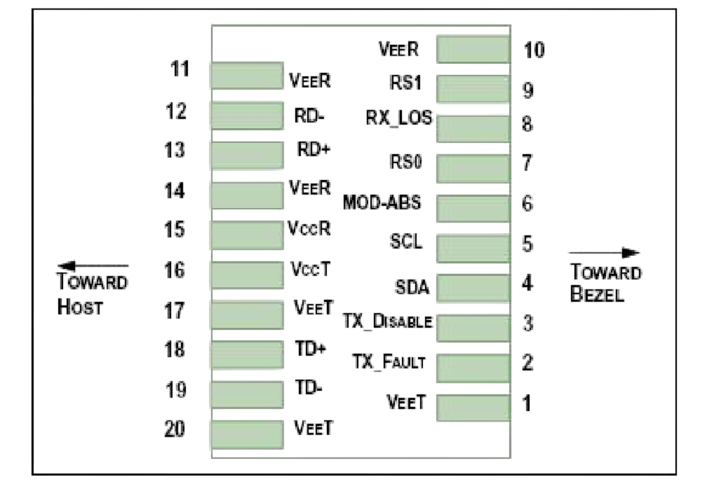
Pin Assignment
|
Pin |
Logic |
Symbol |
Name/Description |
Note |
|
1 |
|
VeeT |
Module Transmitter Ground |
|
|
2 |
LVTTL-O |
TX_Fault |
Module Transmitter Fault |
|
|
3 |
LVTTL-I |
TX_Disable |
Transmitter Disable; Turns off transmitter laser output |
|
|
4 |
LVTTL-I/O |
SDA |
2-wire Serial Interface Data Line (Same as MOD-DEF2 as defined in the INF-8074i) |
|
|
5 |
LVTTL-I/O |
SCL |
2-wire Serial Interface Clock (Same as MOD-DEF1 as defined in the INF-8074i) |
|
|
6 |
|
MOD_ABS |
Module Absent, connected to VeeT or VeeR in the module |
|
|
7 |
LVTTL-I |
RS0 |
Not used |
|
|
8 |
LVTTL-O |
RX_LOS |
Receiver Loss of Signal Indication (In FC designated as RX_LOS, in SONET designated as LOS, and in Ethernet designated at Signal Detect) |
|
|
9 |
LVTTL-I |
RS1 |
Not used |
|
|
10 |
|
VeeR |
Module Receiver Ground |
|
|
11 |
|
VeeR |
Module Receiver Ground |
|
|
12 |
CML-O |
RD- |
Receiver Inverted Data Output |
|
|
13 |
CML-O |
RD+ |
Receiver Non-Inverted Data Output |
|
|
14 |
|
VeeR |
Module Receiver Ground |
|
|
15 |
|
VccR |
Module Receiver 3.3 V Supply |
|
|
16 |
|
VccT |
Module Transmitter 3.3 V Supply |
|
|
17 |
|
VeeT |
Module Transmitter Ground |
|
|
18 |
CML-I |
TD+ |
Transmitter Non-Inverted Data Input |
|
|
19 |
CML-I |
TD- |
Transmitter Inverted Data Input |
|
|
20 |
|
VeeT |
Module Transmitter Ground |
|
If you need more support , Please contact us.

