

Click to open expanded view
1.25Gb/s SFP CWDM 100km
Product Features
Hot-Pluggable
Duplex LC connector
Single +3.3V Power Supply
Up to 1.25Gb/s Data Links
CWDM DFB laser transmitter
Up to 100km on 9/125μm SMF
Low power dissipation <1W typically
18-Wavelength CWDM 1270n~1610nm Available
Monitoring Interface Compliant with SFF-8472
Operating temperature range: 0°C to 70°C
RoHS compliant and Lead Free
Applications
2Gigabit Ethernet
1XFiber Channel
CWDM Networks
Description
This transceiver provide optical networking equipment manufacturers with a timely and cost effective tool in supporting the unceasing demand for higher bandwidth equipment build-outs in the enterprise access and metropolitan area networks. There are 18 center wavelengths available from 1270nm to 1610nm. The 20nm channel spacing allows for un-cooled laser operation, a high yield manufacturing process, and lower cost Mux/Demux technology, thus providing a complete cost effective solution for various data and telecom applications.
Absolute Maximum Ratings
Table 1-Absolute Maximum Ratings
|
Parameter |
Symbol |
Min |
Max |
Unit |
Note |
|
Storage Temperature |
TS |
-40 |
85 |
°C |
|
|
Operating Case Temperature |
TOP |
0 |
70 |
°C |
|
|
Power Supply Voltage |
VCC |
-0.5 |
3.6 |
V |
|
|
Relative Humidity (non-condensation) |
RH |
0 |
85 |
% |
|
Note:
It has to be noted that the operation in excess of any individual absolute maximum ratings might cause permanent damage to this module.
Recommended Operating Conditions
Table 2-Recommended Operating Conditions
|
Parameter |
Symbol |
Min |
Typical |
Max |
Unit |
Note |
|
Operating Case Temperature |
TOP |
0 |
|
70 |
°C |
|
|
Power Supply Voltage |
VCC |
3.135 |
3.3 |
3.465 |
V |
|
|
Power Consumption |
P |
|
|
1 |
W |
|
|
Supply Current |
Icc |
|
|
300 |
mA |
|
|
Bit Error Rate |
BER |
|
|
10-12 |
|
|
|
Aggregate Bit Rate |
BRAVE |
- |
1.25 |
- |
Gb/s |
|
|
Transmission Distance |
TD |
|
- |
100 |
KM |
Over SMF |
Optical Characteristics
Table 3-Optical Characteristics
|
Transmitter Optical Specification |
||||||
|
Parameter |
Symbol |
Min |
Typ |
Max |
Units |
Notes |
|
Center Wavelength |
λc |
λ-6.5 |
λ |
λ+6.5 |
nm |
|
|
Spectral Width |
σ |
|
|
1 |
nm |
|
|
Side Mode Suppression Ratio |
SMSR |
30 |
|
|
dB |
|
|
Optical Output Power |
Pout |
-1 |
|
+5 |
dBm |
|
|
Optical Rise/Fall Time |
tr / tf |
|
|
260 |
ps |
|
|
Extinction Ratio |
ER |
8.2 |
|
|
dB |
|
|
Generated Jitter (peak to peak) |
JTXp-p |
|
|
0.07 |
UI |
|
|
Generated Jitter (rms) |
JTXrms |
|
|
0.007 |
UI |
|
|
Eye Mask for Optical Output |
|
Compliant with IEEE802.3z(class 1 laser safety) |
|
|
||
|
Receiver Optical Specification |
||||||
|
Optical Input Wavelength |
λc |
1260 |
|
1620 |
nm |
|
|
Receiver Overload |
Pol |
-3 |
|
|
dBm |
|
|
RX Sensitivity |
Sen |
|
|
-28 |
dBm |
|
|
RX_LOS Assert |
LOS A |
-45 |
|
|
dBm |
|
|
RX_LOS De-assert |
LOS D |
|
|
-29 |
dBm |
|
|
RX_LOS Hysteresis |
LOS H |
0.5 |
|
|
dB |
|
Electrical Characteristics
The following electrical characteristics are defined over the recommended operating environment
Table 4-Electrical Characteristics
|
Parameter |
Symbol |
Mi |
Typ |
Max |
Units |
Notes |
|
|
Transmitter (Module Input) |
|||||||
|
Input differential impedance |
Rin |
90 |
100 |
110 |
|
|
|
|
Single ended data input swing |
Vin PP |
250 |
|
1200 |
mVp-p |
1 |
|
|
Transmit Disable Voltage |
VD |
Vcc – 1.3 |
|
Vcc |
V |
2 |
|
|
Transmit Enable Voltage |
VEN |
Vee |
|
Vee+ 0.8 |
V |
|
|
|
Transmit Disable Assert Time |
Tdessert |
|
|
10 |
us |
|
|
|
Receiver (Module Output) |
|||||||
|
Single ended data output swing |
Vout,pp |
300 |
|
800 |
mv |
3 |
|
|
Data output rise time |
tr |
|
|
260 |
ps |
4 |
|
|
Data output fall time |
tf |
|
|
260 |
ps |
4 |
|
|
LOS Fault |
Vlosfault |
Vcc – 0.5 |
|
VCC_host |
V |
5 |
|
|
LOS Normal |
Vlos norm |
Vee |
|
Vee+0.5 |
V |
5 |
|
|
Power Supply Rejection |
PSR |
100 |
|
|
mVpp |
6 |
|
|
|
|
|
|
|
|
|
|
Note:
1、AC coupled.
2、Or open circuit.
3、Into 100 ohm differential termination. 4. 20 – 80 %
4、LOS is LVTTL. Logic 0 indicates normal operation; logic 1 indicates no signal detected.
5、All transceiver specifications are compliant with a power supply sinusoidal modulation of 20 Hz to 1.5MHz up to specified value applied through the power supply filtering network shown on page 23 of the Small Form-factor Pluggable (SFP) Transceiver Multi-Source Agreement (MSA), September 14, 2000.
Digital Diagnostics
Table 6-Digital Diagnostics
|
Parameter |
Symbol |
Min |
Max |
Unit |
Note |
|
Temperature Monitor Absolute Error |
DMI_Temp |
-3 |
3 |
°C |
Cover full operating temperature range |
|
Supply Voltage Monitor Absolute Error |
DMI _VCC |
-0.1 |
0.1 |
V |
Cover full operating temperature range |
|
Channel RX Power Monitor Absolute Error |
DMI_RX_Ch |
-3 |
3 |
dB |
|
|
Channel Bias Current Monitor |
DMI_Ibias_Ch |
-10% |
10% |
|
|
|
Channel TX Power Monitor Absolute Error |
DMI_TX_Ch |
-3 |
3 |
dB |
|
Edge connector and pinout description
The electrical pinout of the SFP module is shown in Figure below.
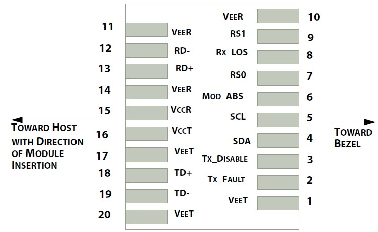
|
PIN # |
Name |
Function |
Notes |
|
1 |
VeeT |
1 |
|
|
2 |
Tx Fault |
2 |
|
|
3 |
Tx Disable |
Transmitter Disable – High or open disables the transmitter |
|
|
4 |
SDL |
2-wire Serial Interface Data Line (MOD-DEF2) |
3 |
|
5 |
SCL |
2-wire Serial Interface Clock (MOD-DEF1) |
3 |
|
6 |
MOD-ABS |
Module Absent, connected to VeeT or VeeR in the module |
|
|
7 |
RS0 |
Rate Select 0 |
5 |
|
8 |
RX_LOS |
Receiver Loss of Signal(LVTTL-O). Logic 0 indicates normal operation |
4 |
|
9 |
RS1 |
Rate Select 1 |
1 |
|
10 |
VeeR |
Receiver Ground |
1 |
|
11 |
VeeR |
1 |
|
|
12 |
RD- |
Inverse Received Data out (CML-O), AC Coupled |
|
|
13 |
RD+ |
Receiver Non-inverted DATA out. AC Coupled |
|
|
14 |
VeeR |
Receiver Ground |
1 |
|
15 |
VccR |
Receiver Power Supply |
|
|
16 |
VccT |
Transmitter Power Supply |
|
|
17 |
VeeT |
Transmitter Ground |
1 |
|
18 |
TD+ |
Transmitter Non-Inverted DATA in. AC Coupled. |
|
|
19 |
TD- |
Transmitter Inverted DATA in. AC Coupled. |
|
|
20 |
VeeT |
Transmitter Ground |
1 |
If you need more support , Please contact us .
