
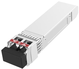
Click to open expanded view
Features
Single 3.3V Power supply
Power Dissipation < 1.5W
Duplex LC Connector Interface
Hot-Pluggable SFP28 Form Factor
Distance up to 40km with 9/125µm SMF
1310nm DFB Transmitter /APD-TIA Receiver
Digital diagnostics functions are available via the I2C interface
Operating data rate support 24.33Gbps and 25.78Gbps with CDR engaged mode
Operating data rate support 9.95Gbps and 10.31Gbps with CDR bypassed mode
Operating Case Temperature: Commercial: 0℃ ~ +70℃,Industrial: -40℃ ~ +85℃
Applications
Other Optical Links
25GBASE-ER Ethernet
5G front haul CPRI10, eCPRI10
Standard
Compliant with IEEE 802.3cc
Compliant with MSA SFF-8402, SFF-8432, SFF-8431& SFF-8472
Order Information
|
Part No. |
Package |
Data Rate |
Fiber |
Distance |
Interface |
Temp. |
DDMI |
|
HC-25-40-13-I |
SFP28 |
Up to 25.78Gbps |
SMF |
40km |
Duplex LC |
-40~85℃ |
YES |
Optical Characteristics
|
Parameter |
Symbol |
Min. |
Typ. |
Max. |
Unit |
|
Transmitter |
|||||
|
Center Wavelength Spacing |
|
1290 |
1310 |
1330 |
GHz |
|
Spectral Width (-20dB) |
∆λ |
|
|
1 |
nm |
|
Average Output Power*(Note1) |
Pout |
0 |
|
5 |
dBm |
|
Extinction Ratio |
ER |
3.0 |
|
|
dB |
|
Average Power of OFF Transmitter |
Poff |
|
|
-30 |
dBm |
|
Relative Intensity Noise |
RIN |
|
|
-128 |
dB/Hz |
|
Side Mode Suppression Ratio |
SMSR |
30 |
|
|
dB |
|
Transmitter Dispersion Penalty |
TDP |
|
|
3 |
dB |
|
TX_Disable Assert Time |
T_off |
- |
- |
10 |
us |
|
Receiver |
|||||
|
Center Wavelength |
λC |
1260 |
λ |
1600 |
nm |
|
Receive Sensitivity OMA*(Note2) |
Pmin |
|
|
-18 |
dBm |
|
Receiver Overload |
Pmax |
-6 |
|
|
dBm |
|
LOS De-Assert |
LOSD |
|
|
-19 |
dBm |
|
LOS Assert |
LOSA |
-36 |
|
|
dBm |
|
LOS-Hysteresis |
Phys |
0.5 |
|
|
dB |
Note:
1) Output is coupled into a 9/125um SMF.
2) Sensitivity tested at 25.78Gbps 5.0x10⁻⁵ BER.
Electrical Characteristics
|
Parameter |
Symbol |
Min. |
Typ. |
Max. |
Unit |
Notes |
|
|
Transmitter |
|||||||
|
Differential data input swing |
Vin |
150 |
|
1200 |
mVpp |
AC Coupled Inputs |
|
|
Input AC Common Mode Voltage |
|
0 |
|
25 |
mV |
RMS |
|
|
Input Impedance (Differential) |
Zin |
85 |
100 |
115 |
ohms |
Rin > 100 kohms @ DC |
|
|
TX_DIS |
High |
|
2 |
|
Vcc |
V |
|
|
Low |
|
0 |
|
0.8 |
|
||
|
TX_FAULT |
High |
|
2 |
|
Vcc+0.3 |
V |
lo = 400μA; Host Vcc |
|
Low |
|
0 |
|
0.5 |
lo = -4.0mA |
||
|
Receiver |
|||||||
|
CML Outputs (Differential) |
Vout |
350 |
|
700 |
mVpp |
AC Coupled Outputs |
|
|
Output Impedance (Differential) |
Zout |
85 |
100 |
115 |
ohms |
|
|
|
|
|
|
|
|
|
|
|
|
RX_LOS |
High |
|
2 |
|
Vcc+0.3 |
|
lo = 400μA; Host Vcc |
|
Low |
|
0 |
|
0.8 |
lo = -4.0mA |
||
|
MOD_DEF (0.2) |
VoH |
2.5 |
|
|
V |
With Serial ID |
|
|
VoL |
0 |
|
0.5 |
||||
Absolute Maximum Ratings
|
Parameter |
Symbol |
Min. |
Max. |
Unit |
|
Storage Temperature |
Ts |
-40 |
+85 |
°C |
|
Maximum Supply Voltage |
VCC |
-0.5 |
3.6 |
V |
|
Operating Relative Humidity (non-condensing) |
RH |
5 |
85 |
% |
Note:
Exceeding any one of these values may destroy the device permanently.
Recommended Operating Conditions
|
Parameter |
Symbol |
Min. |
Typ. |
Max. |
Unit |
|
Operating Case Temperature |
TC |
-40 |
|
+85 |
℃ |
|
Power Supply Voltage |
VCC |
3.13 |
3.3 |
3.47 |
V |
|
Power Supply Current |
ICC |
|
|
450 |
mA |
Digital Diagnostic Functions
25G SFP28 transceivers provide an enhanced digital diagnostic.
|
Parameter |
Range |
Unit |
Accuracy |
Calibration |
|
Temperature |
-40 to +85 |
°C |
±3°C |
Internal |
|
Voltage |
3.13 to 3.47 |
V |
±3% |
Internal |
|
Bias Current |
10 to 85 |
mA |
±10% |
Internal |
|
TX Power |
0 to 5 |
dBm |
±3dB |
Internal |
|
RX Power |
-18 to -6 |
dBm |
±3dB |
Internal |
Note:
The transceivers provide serial ID memory contents and diagnostic information about the present operating conditions by the 2-wire serial interface (SCL, SDA). The diagnostic information with internal calibration or external calibration all are implemented, including received power monitoring, transmitted power monitoring,bias current monitoring, supply voltage monitoring and temperature monitoring.
Electrical Pin-out Details
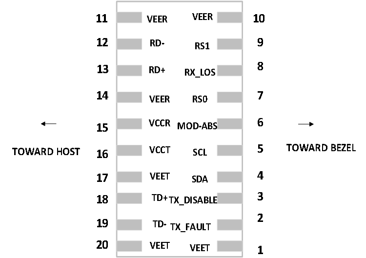
Pin Function Definitions
|
Pin |
Name |
Function |
Plug Seq. |
Notes |
|
1 |
VeeT |
Transmitter Ground |
1 |
5) |
|
2 |
TX Fault |
Transmitter Fault Indication |
3 |
1) |
|
3 |
TX Disable |
Transmitter Disable |
3 |
2) Module disables on high or open |
|
4 |
SDA |
Transmitter Disable |
3 |
3) 2 wire serial ID interface. |
|
5 |
SCL |
Module Definition 2 |
3 |
3) 2 wire serial ID interface. |
|
6 |
MOD-ABS |
Module Definition 1 |
3 |
3) |
|
7 |
RS0 |
RX Rate Select (LVTTL). |
3 |
9) |
|
8 |
LOS |
Loss of Signal |
3 |
4) |
|
9 |
RS1 |
TX Rate Select (LVTTL). |
1 |
9) |
|
10 |
VeeR |
Receiver Ground |
1 |
5) |
|
11 |
VeeR |
Receiver Ground |
1 |
5) |
|
12 |
RD- |
Inv. Received Data Out |
3 |
6) |
|
13 |
RD+ |
Received Data Out |
3 |
6) |
|
14 |
VeeR |
Receiver Ground |
1 |
5) |
|
15 |
VccR |
Receiver Power |
2 |
7) 3.3V ± 5% |
|
16 |
VccT |
Transmitter Power |
2 |
7) 3.3V ± 5% |
|
17 |
VeeT |
Transmitter Ground |
1 |
5) |
|
18 |
TD+ |
Transmit Data In |
3 |
8) |
|
19 |
TD- |
Inv. Transmit Data In |
3 |
8) |
|
20 |
VeeT |
Transmitter Ground |
1 |
5) |
NOTES:
1) TX Fault is an open collector/drain output, which should be pulled up with a 4.7K-10K resistor on the host
board. When high, output indicates a laser fault of some kind. Low indicates normal operation. In the low state, the output will be pulled to < 0.8V.
2) TX disable is an input that is used to shut down the transmitter optical output. It is pulled up within the
module with a 4.7K-10K resistor. It states are:
Low (0-0.8V): Transmitter on
(>0.8, < 2.0V): Undefined
High (2.0 – 3.465V): Transmitter Disabled
Open: Transmitter Disabled
3) Modulation Absent, connected to VEET or VEER in the module.
4) LOS (Loss of Signal) is an open collector/drain output, which should be pulled up with a 4.7K-10K resistor.
When high, this output indicates the received optical power is below the worst-case receiver Sensitivity (as defined by the Standard in use). Low indicates normal operation in the low state, the output will be pulled to < 0.8V.
5) VeeR and VeeT may be internally connected within the SFP module.
6) RD-/+: These are the differential receiver outputs. They are AC coupled 100Ω differential Lines which should
be terminated with 100Ω (differential) at the user SERDES.
7) VccR and VccT are the receiver and transmitter power supplies. They are defined as 3.3V±5% at the SFP
connector pin.
8) TD-/+: These are the differential transmitter inputs. They are AC-coupled,differential lines with 100Ω
differential termination inside the module.
9) CDR control(Volatile parameter. Reset to default value on boot).
|
|
Hard PIN7 |
Soft RS0 Bit,A2H Byte 110d bit3 |
Mode of Operation |
|
RS0 |
0 |
0 |
Rx:9.8304Gb/s,10.1376Gb/s or 10.3125Gb/s |
|
0 |
1(default) |
Rx:24.33024Gb/s or 25.78125Gb/s. Module auto detect data rate and CDR lock accordingly. |
|
|
1 |
0 |
||
|
1 |
1(default) |
||
|
|
Hard PIN9 |
Soft RS1 Bit,A2H Byte 118d bit3 |
Mode of Operation |
|
RS1 |
0 |
0 |
Tx:9.8304Gb/s,10.1376Gb/s or 10.3125Gb/s |
|
0 |
1(default) |
Tx:24.33024Gb/s or 25.78125Gb/s. Module auto detect data rate and |
|
|
1 |
0 |
||
|
1 |
1(default) |
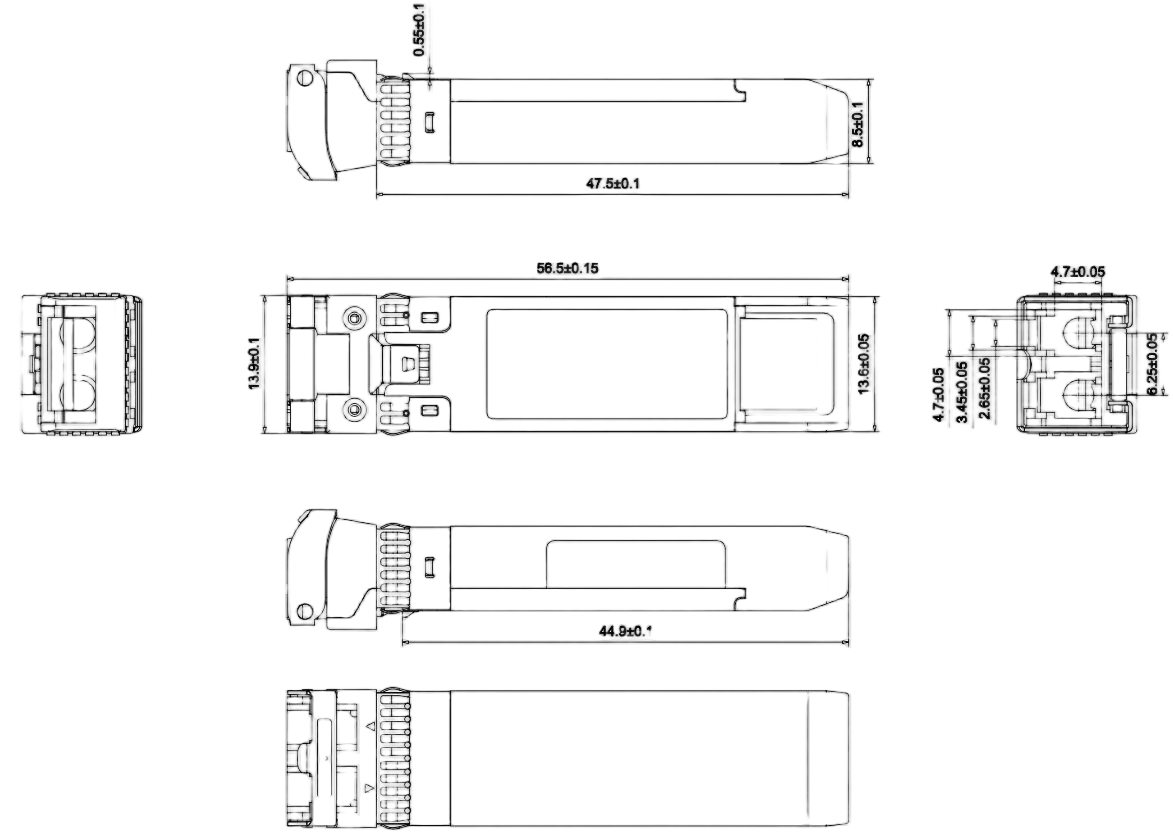
Mechanical Specifications
If you need more support , Please contact us .

