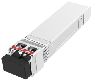
Click to open expanded view
Features
Operating Data Rate up to 25.78Gbps
1310nm DFB Transmitter /PIN-TIA Receiver
Distance up to 10km with 9/125µm SMF
Single 3.3V Power supply
Hot-Pluggable SFP28 Footprint
Duplex LC Connector Interface
Power Dissipation < 1.5W
Digital diagnostics functions are available via the I2C interface
Operating Case Temperature:
Commercial: 0℃ ~ +70℃
Industrial: -40℃ ~ +85℃
Applications
25GBASE-LR Ethernet
5G front haul CPRI10, eCPRI10
Other Optical Links
Standard
Compliant with MSA SFF-8402, SFF-8432, SFF-8431& SFF-8472
Compliant with IEEE 802.3cc
Order Information
|
Part No. |
Package |
Data Rate |
Fiber |
Distance |
Interface |
Temp. |
DDMI |
|
HC-25-10-13-I |
SFP28 |
Up to 25.78Gbps |
SMF |
10km |
Duplex LC |
-40~85℃ |
YES |
Optical Characteristics
|
Parameter |
Symbol |
Min. |
Typ. |
Max. |
Unit |
|
Transmitter |
|||||
|
Center Wavelength Spacing |
|
1290 |
1310 |
1330 |
GHz |
|
Spectral Width (-20dB) |
∆λ |
|
|
1 |
nm |
|
Average Output Power*(Note1) |
Pout |
-4 |
|
2 |
dBm |
|
Extinction Ratio |
ER |
3.5 |
|
|
dB |
|
Average Power of OFF Transmitter |
Poff |
|
|
-20 |
dBm |
|
Relative Intensity Noise |
RIN |
|
|
-128 |
dB/Hz |
|
Side Mode Suppression Ratio |
SMSR |
30 |
|
|
dB |
|
Transmitter Dispersion Penalty |
TDP |
|
|
3 |
dB |
|
TX_Disable Assert Time |
T_off |
- |
- |
10 |
us |
|
Receiver |
|||||
|
Center Wavelength |
λC |
1260 |
|
1600 |
nm |
|
Receive Sensitivity OMA*(Note2) |
Pmin |
|
|
-12 |
dBm |
|
Receiver Overload |
Pmax |
3 |
|
|
dBm |
|
LOS De-Assert |
LOSD |
|
|
-14 |
dBm |
|
LOS Assert |
LOSA |
-30 |
|
|
dBm |
|
LOS-Hysteresis |
Phys |
0.5 |
|
|
dB |
Note:
1) Output is coupled into a 9/125um SMF.
2) Sensitivity tested at 25.78Gbps 5.0x10⁻⁵ BER.
Electrical Characteristics
|
Parameter |
Symbol |
Min. |
Typ. |
Max. |
Unit |
Notes |
|
|
Transmitter |
|||||||
|
Differential data input swing |
Vin |
150 |
|
1200 |
mVpp |
AC Coupled Inputs |
|
|
Input AC Common Mode Voltage |
|
0 |
|
25 |
mV |
RMS |
|
|
Input Impedance (Differential) |
Zin |
85 |
100 |
115 |
ohms |
Rin > 100 kohms @ DC |
|
|
TX_DIS |
High |
|
2 |
|
Vcc |
V |
|
|
Low |
|
0 |
|
0.8 |
|
||
|
TX_FAULT |
High |
|
2 |
|
Vcc+0.3 |
V |
lo = 400μA; Host Vcc |
|
Low |
|
0 |
|
0.5 |
lo = -4.0mA |
||
|
Receiver |
|||||||
|
CML Outputs (Differential) |
Vout |
350 |
|
700 |
mVpp |
AC Coupled Outputs |
|
|
Output Impedance (Differential) |
Zout |
85 |
100 |
115 |
ohms |
|
|
|
RX_LOS |
High |
|
2 |
|
Vcc+0.3 |
|
lo = 400μA; Host Vcc |
|
Low |
|
0 |
|
0.8 |
lo = -4.0mA |
||
|
MOD_DEF (0.2) |
VoH |
2.5 |
|
|
V |
With Serial ID |
|
|
VoL |
0 |
|
0.5 |
||||
Absolute Maximum Ratings
|
Parameter |
Symbol |
Min. |
Max. |
Unit |
|
Storage Temperature |
Ts |
-40 |
+85 |
°C |
|
Maximum Supply Voltage |
VCC |
-0.5 |
3.6 |
V |
|
Operating Relative Humidity (non-condensing) |
RH |
5 |
85 |
% |
Note:
Exceeding any one of these values may destroy the device permanently.
Recommended Operating Conditions
|
Parameter |
Symbol |
Min. |
Typ. |
Max. |
Unit |
|
Operating Case Temperature |
Tc |
-40 |
|
+85 |
°C |
|
Power Supply Voltage |
Vcc |
3.13 |
3.3 |
3.47 |
V |
|
Power Supply Current |
Icc |
|
|
450 |
|
 mA
mA
Digital Diagnostic Functions
25G SFP28 transceivers provide an enhanced digital diagnostic.
|
Parameter |
Range |
Unit |
Accuracy |
Calibration |
|
Temperature |
-40 to 85 |
°C |
±3°C |
Internal |
|
Voltage |
3.13 to 3.47 |
V |
±3% |
Internal |
|
Bias Current |
15 to 85 |
mA |
±10% |
Internal |
|
TX Power |
-4 to 2 |
dBm |
±3dB |
Internal |
|
RX Power |
-12 to 3 |
dBm |
±3dB |
Internal |
Note:
The transceivers provide serial ID memory contents and diagnostic information about the present operating conditions by the 2-wire serial interface (SCL, SDA). The diagnostic information with internal calibration or external calibration all are implemented, including received power monitoring, transmitted power monitoring,
bias current monitoring, supply voltage monitoring and temperature monitoring.
Electrical Pin-out Details
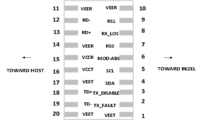
Pin Function Definitions
|
Pin |
Name |
Function |
Plug Seq. |
Notes |
|
1 |
VeeT |
Transmitter Ground |
1 |
5) |
|
2 |
TX Fault |
Transmitter Fault Indication |
3 |
1) |
|
3 |
TX Disable |
Transmitter Disable |
3 |
2) Module disables on high or open |
|
4 |
SDA |
Transmitter Disable |
3 |
3) 2 wire serial ID interface. |
|
5 |
SCL |
Module Definition 2 |
3 |
3) 2 wire serial ID interface. |
|
6 |
MOD-ABS |
Module Definition 1 |
3 |
3) |
|
7 |
RS0 |
RX Rate Select (LVTTL). |
3 |
NC (Pin not used) |
|
8 |
LOS |
Loss of Signal |
3 |
4) |
|
9 |
RS1 |
TX Rate Select (LVTTL). |
1 |
NC (Pin not used) |
|
10 |
VeeR |
Receiver Ground |
1 |
5) |
|
11 |
VeeR |
Receiver Ground |
1 |
5) |
|
12 |
RD- |
Inv. Received Data Out |
3 |
6) |
|
13 |
RD+ |
Received Data Out |
3 |
6) |
|
14 |
VeeR |
Receiver Ground |
1 |
5) |
|
15 |
VccR |
Receiver Power |
2 |
7) 3.3V ± 5% |
|
16 |
VccT |
Transmitter Power |
2 |
7) 3.3V ± 5% |
|
17 |
VeeT |
Transmitter Ground |
1 |
5) |
|
18 |
TD+ |
Transmit Data In |
3 |
8) |
|
19 |
TD- |
Inv. Transmit Data In |
3 |
8) |
|
20 |
VeeT |
Transmitter Ground |
1 |
5) |
NOTES:
1) TX Fault is an open collector/drain output, which should be pulled up with a 4.7K-10K resistor on the host
board. When high, output indicates a laser fault of some kind. Low indicates normal operation. In the low state, the output will be pulled to < 0.8V.
2) TX disable is an input that is used to shut down the transmitter optical output. It is pulled up within the
module with a 4.7K-10K resistor. It states are:
Low (0-0.8V): Transmitter on
(>0.8, < 2.0V): Undefined
High (2.0 – 3.465V): Transmitter Disabled
Open: Transmitter Disabled
3) Modulation Absent, connected to VEET or VEER in the module.
4) LOS (Loss of Signal) is an open collector/drain output, which should be pulled up with a 4.7K-10K resistor.
When high, this output indicates the received optical power is below the worst-case receiver Sensitivity (as defined by the Standard in use). Low indicates normal operation in the low state, the output will be pulled to < 0.8V.
5) VeeR and VeeT may be internally connected within the SFP module.
6) RD-/+: These are the differential receiver outputs. They are AC coupled 100Ω differential Lines which should
be terminated with 100Ω (differential) at the user SERDES.
7) VccR and VccT are the receiver and transmitter power supplies. They are defined as 3.3V±5% at the SFP
connector pin.
8) TD-/+: These are the differential transmitter inputs. They are AC-coupled,differential lines with 100Ω
differential termination inside the module.EEPROM
The serial interface uses the 2-wire serial CMOS EEPROM protocol defined. When the serial protocol is activated, the host generates the serial clock signal (SCL). The positive edge clocks data into those segments of the EEPROM that are not write protected within the SFP transceiver. The negative edge clocks data from the SFP transceiver. The serial data signal (SDA) is Bi-directional for serial data transfer. The host uses SDA in conjunction with SCL to mark the start and end of serial protocol activation. The memories are organized as a series of 8-bit data words that can be addressed individually or sequentially. The Module provides diagnostic information about the present operating conditions. The transceiver generates this diagnostic data by digitization of internal analog signals. Calibration and alarm/warning threshold data is written during device manufacture. Received power monitoring, transmitted power monitoring, bias current monitoring, supply voltage monitoring and temperature monitoring all are implemented. If the module is defined as external calibrated, the diagnostic data are raw A/D values and must be converted to real world units using calibration constants stored in EEPROM locations56 – 95 at wire serial bus address A2h. The digital diagnostic memory map specific data field define as following.
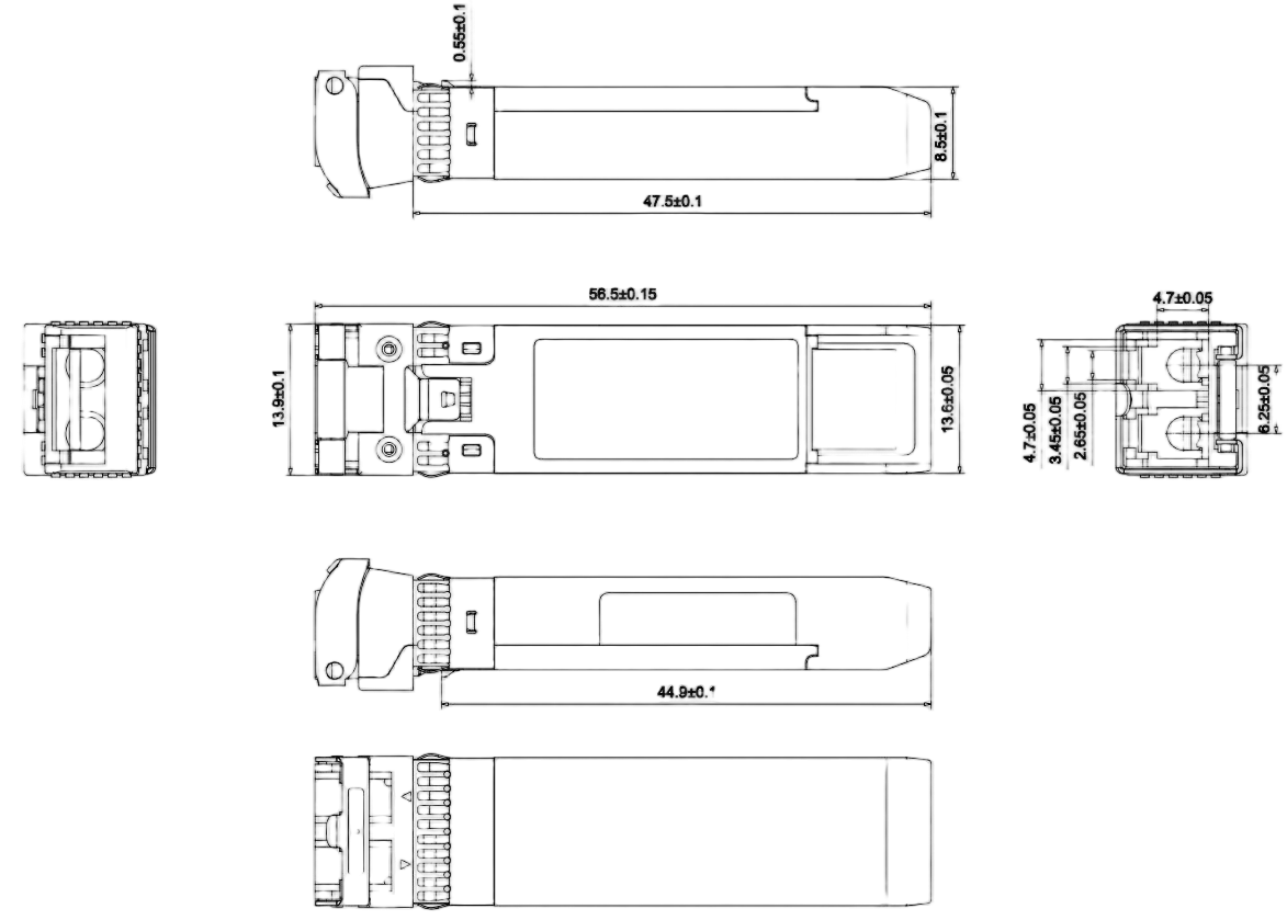
Mechanical Dimensions